Getting to Know Your Hardware
Connections for input/output signals on the PDQ Board Lite 9S12 development board,
including communications, analog, digital, and timer lines.
The PDQ Board Lite, a lower cost version of the PDQ Board, is intended as a development platform for instrument controllers. To that end, it includes a healthy subset of the I/O signals available on the PDQ Board, plus a prototyping area for custom electronic circuitry and a standard Micro-USB power jack.
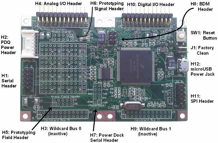
Headers

| PDQ Board Lite Headers and Jumpers | |
|---|---|
| Designator | Function |
| H1 | Serial connector (see the pinout below) RS232 signals (/TxD1, /RxD1, /TxD2, /RxD2 and GND) are the same as for the PDQ Board Logic level RS232 signals are brought out: TxD1 (pin 5), RxD1 (pin 6), TxD2 (pin 10), and RxD2 (pin 4) RS485 signals (XCV1+, XCV1-, XCV2+, XCV2-) are not provided |
| H2 | PDQ Board power connector (Not installed - pinout) Only V+RAW (pin 1), GND (pin 2) and +5V (pin 3) are connected V+RAW is not used by the PDQ Board Lite, but it is passed through to the Analog I/O Connector (H4) |
| H3 | Wildcard Header 0 (Not installed - pinout) Only +5V, V+Raw and GND are connected V+RAW is not used by the PDQ Board Lite, but it is passed through to the Analog I/O Connector (H4) |
| H4 | Analog I/O connector (pinout) Signals are the same as for the PDQ Board |
| H5 | Prototyping field header (see below) unassigned 10-pin header for custom circuitry |
| H6 | Prototyping signal header (see below) brings out 8 IO signals, +5V and GND for custom circuitry |
| H7 | PowerDock Comm header (Not installed - pinout) Mirrors H1 except for no-connects at pins 4,10 |
| H8 | BDM connector (pinout) Signals are the same as for the PDQ Board |
| H9 | Wildcard Header 1 (Not installed - pinout) Only +5V, V+Raw and GND are connected V+RAW is not used by the PDQ Board Lite, but it is passed through to the Analog I/O Connector (H4) |
| H10 | Digital I/O connector (pinout) Signals are the same as for the PDQ Board; two logic-level serial ports available using the Software UART library. |
| H11 | SPI connector (pinout) Signals at pins 1-9 are the same as for the PDQ Board; pin 10 connects to +5V |
| H12 | Power input (USB micro-B) connector (see below) Pin 1 connects to +5V, Pin 5 to GND; pins 2,3,4 connected to nearby holes for custom use. |
| SW1 | Reset Pressing this button causes a hard reset. |
| J1 | Factory cleanup Puts the PDQ Board into special cleanup mode on the next power-up or reset. To return the PDQ Board to its pristine, right-from-the-factory condition, install this jumper, press the Reset Button, and then remove the jumper. Factory cleanup removes any autostart vectors and returns the PDQ Board Lite to its default software configuration. |
Note that the jumper designated J1, next to the reset button, should not normally have a jumper cap installed. It is used only for factory cleaning the board.
H5: Prototyping Custom Field Header
The H5 holes are intended for attaching a custom header to provide an external interface for custom circuitry in the prototyping area. The are not connected to any signals on the PDQ Board Lite, and are available for any custom external connections needed.
H6: Prototyping Signal Header
These holes mirror a handful of digital and analog signals to simplify common needs for custom circuitry in the prototyping area.
| Signal | Pins | Signal | |
|---|---|---|---|
| PP1/PWM1 | —1 | 2— | PP0/PWM0 |
| PT1/IOC1 | —3 | 4— | PT0/IOC0 |
| GND | —5 | 6— | +5V |
| AN1 | —7 | 8— | AN0 |
| AN3 | —9 | 10— | AN2 |
H12: Micro-USB Power Socket
Only +5V and GND are connected to the PDQ Board Lite. The three data signals from this connector are routed to holes near the connector for forward compatibility.
| Pins | Signal |
|---|---|
| 1— | +5V |
| 2— | Data+ |
| 3— | Data- |
| 4— | ID/NC |
| 5— | GND |
The schematics provide the full pinouts for all of the headers on the PDQ Board Lite.
Dual standard and logic level RS232 serial ports
The PDQ Board Lite brings out two RS232 serial ports to a 10-pin comm (communications) header (designated H1). The standard RS232 signals are logically inverted and swing at approximately ±9 volts. The transmit and receive signal names are /TxD1 and /RxD1 for serial port 1, and /TxD2 and /RxD2 for serial port 2, where the prepended / indicates logical inversion according to the RS232 standard.
Some modern low cost devices interface via logic level RS232, meaning that at the hardware level the signals are not logically inverted, and the signal levels are +5 volts and ground (instead of +/-9V). The transmit and receive signal names for the logic level serial ports are TxD1 and RxD1 for serial port 1, and TxD2 and RxD2 for serial port 2. These signals appear on the comm header, replacing the RS485 signals that are not implemented on the PDQ Board Lite.
For example, when serial port 1 is in its idle state, the standard /TxD1 signal will be at approximately -9 volts, while the corresponding logic level signal TxD1 will be idling at +5V; this is known as a mark condition according to the RS232 standard. During a space bit, the /TxD1 signal is approximately +9 volts, while the corresponding logic level TxD1 signal is about 0 volts.
The following table shows the RS232 signals available on the H1 communications header:
| H1: Communications Header | |||
|---|---|---|---|
| Signal | Pins | Signal | |
| /TxD1 | – 1 | 2 – | /RxD1 |
| DGND | – 3 | 4 – | RxD2 |
| TxD1 | – 5 | 6 – | RxD1 |
| /TxD2 | – 7 | 8 – | /RxD2 |
| DGND | – 9 | 10 – | TxD2 |
| Note: <block indent>This pinout differs from that of the PDQ Board comm header; RS485 signals are replaced with logic level RS232 signals.</block> | |||
A third logic-level serial port is available on pins PT4 and PT5 of the Digital I/O Connector. See: Implementing Logic-Level Serial Ports
SPI Master/Slave Configuration
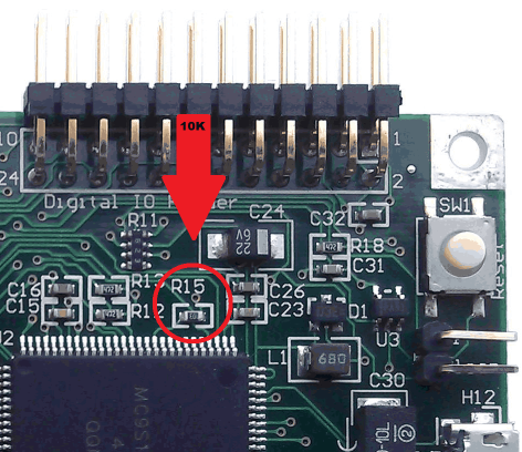
The SPI connector H11 may be used for high-speed communication between two PDQ Boards, regardless of whether one or both are the full PDQ Board or the PDQ Board Lite. By default both boards are configured to be a master on SPI1 and a slave on SPI2. In order to directly connect the boards pin-to-pin, the channels must be switched on the second board, so that it is a slave on SPI1 and a master on SPI2. To configure a PDQ Board Lite as the second board in such a configuration, a 10K surface-mount resistor, package 0603 imperial / 1608 metric, must be installed in position R15 as shown below.
Wildcard interface
The PDQ Board Lite does not have a Wildcard bus, so it does not interface to active Wildcards (that is, Wildcards that are addressed as active devices on the Wildcard bus such as the Analog I/O Wildcard). However, passive Wildcards that don't require access to the processor's control signals may be used, so long as appropriate cables are used to power and connect the Wildcards. Passive Wildcards include the following:
Prototyping area
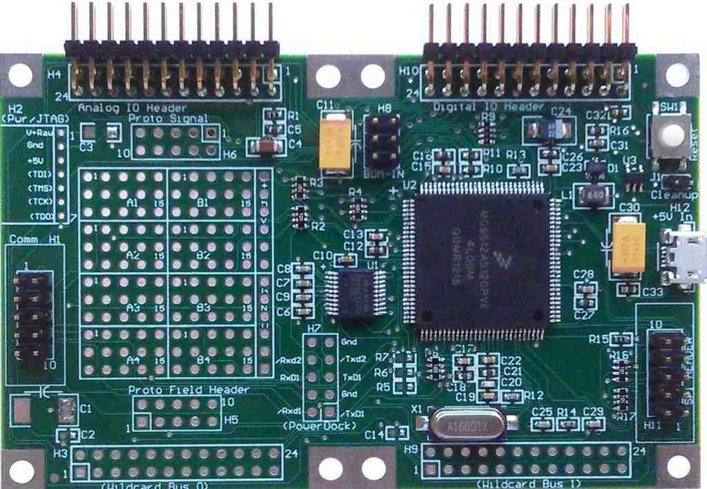
The PDQ Board Lite includes a prototyping area for custom electronic circuitry so that you can customize your controller with specialized I/O. The prototyping area is a sea-of-holes on 0.1" (2.54 mm) centers that can be used to hold DIP (dual in-line package) integrated circuits such as operational amplifiers and logic devices for interfacing to sensors and actuators. There are also 6 holes that bring out +5V and six holes connected to ground to simplify the wiring. The silkscreen clearly labels the holes connected to +5V and GND.
On the top of the sea-of-holes, just below the Analog IO header, is the footprint for a 10-pin labeled H6: Proto Signal (see pinout). This prototyping signal header brings out signals PP1, PP0, PT1 and PT0 on pins 1 - 4 respectively, and signals AN1, AN0, AN3 and AN2 on pins 7 - 10 respectively. Pin 5 is connected to ground, and pin 6 to +5V. This header footprint makes it easy to route these signals to the prototyping circuitry that may be mounted in the sea of holes. Below the sea-of-holes is an uncommitted 10-pin header footprint labeled Proto Field Header. This footprint allows external sensor or actuator lines to be routed to the prototyping area.
To take prototyping circuitry into low volume production, a printed circuit board that includes the signal conditioning circuitry can be laid out with signal and field connections that mate to the PDQ Board Lite at the 10-pin Proto Signal and Proto Field Header locations. For high volume applications, contact Mosaic Industries to discuss the development of a custom board.
Schematics
Here are the schematics of the PDQ Board Lite, providing the pin assignments for the connectors. Note that the only installed connectors are H1 (communications), H4 (analog IO), H8 (BDM, for factory use only), H10 (digital IO), H11 (dual SPI), and H12 (micro-USB power input).
See also → Programming PDQ Board Lite


