I/O Filter Wildcard User Guide
Easily add signal conditioning, filtering, or circuit protection components to any input or output
The I/O Filter Wildcard provides a convenient place for prototyping analog circuitry or for filtering, conditioning or protecting the I/O lines of other Wildcards. Twenty-four I/O lines can be independently filtered, or their signals can be combined in custom ways.
When connecting external signals for data acquisition, you should always filter your input and output lines; this will provide the best reliability and longevity for your instrumentation. Two 24-pin connectors are used for input and output; one generally mates to the field connector of a Wildcard I/O module, while the other connects to your external signals. A third connector accommodates the Wildcard Bus, which can be used for power and ground. Up to four through-hole and four surface-mount components can be soldered onto the board to filter each of the 24 I/O lines.
Connecting to the I/O Filter Wildcard
The I/O Filter Wildcard is a nearly blank prototyping board with a sea of holes for mounting components and three 24-pin headers. The headers/connectors are used as follows:
H1 - Wildcard Bus connector
The Wildcard Bus connector is a 24-pin stacking/go through header/socket that allows the I/O Filter Wildcard to stack on other Wildcards. You can use the power and ground signals on it to power your custom circuitry or to provide signal references.
H2 - I/O (input) connector
H3 - Wildcard Field connector (output)
The Wildcard Field (output) connector is a 24-pin header that you can cable to any other Wildcard Field header. The side of the Wildcard where H3 resides is usually called the front of the Wildcard.
The following table describes the signals on each connector:
| I/O Filter Wildcard Headers | |||||||||||||
|---|---|---|---|---|---|---|---|---|---|---|---|---|---|
| H1 Wildcard Bus | H2 I/O (Input) | H3 Wildcard Field (Output) | |||||||||||
| Signal | Pins | Signal | Signal | Pins | Signal | Signal | Pins | Signal | |||||
| GND | – 1 | 2 – | +5V | Pin 1 I/O | – 1 | 2 – | Pin 2 I/O | Pin 1 I/O | – 1 | 2 – | Pin 2 I/O | ||
| /IRQ | – 3 | 4 – | V+RAW | Pin 3 I/O | – 3 | 4 – | Pin 4 I/O | Pin 3 I/O | – 3 | 4 – | Pin 4 I/O | ||
| PG1 | – 5 | 6 – | PG0 | Pin 5 I/O | – 5 | 6 – | Pin 6 I/O | Pin 5 I/O | – 5 | 6 – | Pin 6 I/O | ||
| MOSI | – 7 | 8 – | MISO | Pin 7 I/O | – 7 | 8 – | Pin 8 I/O | Pin 7 I/O | – 7 | 8 – | Pin 8 I/O | ||
| /RESET | – 9 | 10 – | SCK | Pin 9 I/O | – 9 | 10 – | Pin 10 I/O | Pin 9 I/O | – 9 | 10 – | Pin 10 I/O | ||
| /MOD.CS | – 11 | 12 – | 16 MHz | Pin 11 I/O | – 11 | 12 – | Pin 12 I/O | Pin 11 I/O | – 11 | 12 – | Pin 12 I/O | ||
| E | – 13 | 14 – | R/W | Pin 13 I/O | – 13 | 14 – | Pin 14 I/O | Pin 13 I/O | – 13 | 14 – | Pin 14 I/O | ||
| /OE | – 15 | 16 – | /WE | Pin 15 I/O | – 15 | 16 – | Pin 16 I/O | Pin 15 I/O | – 15 | 16 – | Pin 16 I/O | ||
| AD7 | – 17 | 18 – | AD6 | Pin 17 I/O | – 17 | 18 – | Pin 18 I/O | Pin 17 I/O | – 17 | 18 – | Pin 18 I/O | ||
| AD5 | – 19 | 20 – | AD4 | Pin 19 I/O | – 19 | 20 – | Pin 20 I/O | Pin 19 I/O | – 19 | 20 – | Pin 20 I/O | ||
| AD3 | – 21 | 22 – | AD2 | Pin 21 I/O | – 21 | 22 – | Pin 22 I/O | Pin 21 I/O | – 21 | 22 – | Pin 22 I/O | ||
| AD1 | – 23 | 24 – | AD0 | Pin 23 I/O | – 23 | 24 – | Pin 24 I/O | Pin 23 I/O | – 23 | 24 – | Pin 24 I/O | ||
The greyed-out pins on the Wildcard bus, H1, would not usually be used; only those shown in bold, the power and ground connections, would generally be needed.
If you are filtering inputs to a Wildcard, for each of the 24 I/O lines, you generally apply a signal to H2, the I/O (Input) Connector, you mount custom circuitry on the board to filter the signal, and the filtered signal is delivered to a corresponding pin on H3, the Wildcard Field Connector (Output). If you are conditioning outputs from a Wildcard, then the H3 connector becomes the input to the board, and the H2 connector the output. Of course, if it is more convenient you are free to connect H2 to a Wildcard filed header and H3 to your external devices. Signals may flow in either direction between H2 and H3 – what is important is that there is a one-to-one correspondence between the 24 pins on H2 and H3.
I/O Filter Wildcard circuit schematic
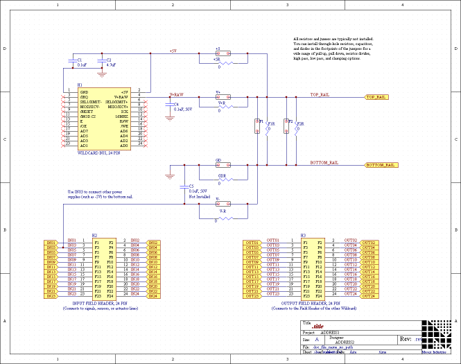
Figure 1 shows the schematic for four of the 24 circuits of the I/O Filter Wildcard; the others are identical. Also shown in Figure 1 are power and ground distribution circuits common to all the 24 channels.
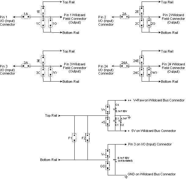
Up to four through-hole or surface-mount components may be connected per circuit, or if both types are used up to eight circuit components may be used as shown below in Figure 2. Some components connect the input pins to the output pins, while other components connect the signal path to either of two rails, a top rail, generally used for the positive power supply, and a bottom rail, generally used for the circuit ground.
Figure 1 also shows several options for deriving the top and bottom rails. The top rail may be connected to the +5V or the V+RAW supplies by jumpering the pads (i.e., connecting a wire or zero ohm resistor) labeled V+ or +5. Similarly, the bottom rail can be connected to the Wildcard Bus ground, but jumpering the GD pads, or to a user supplied input on pin 3 of H2, by jumpering V-. The user supplied input would be generally used if a negative voltage is desired.
These rails may be filtered by using resistors or inductors in place of the zero ohm jumpers and installing capacitors at positions F1 and/or F2. Or they can be protected against overvoltages by installing appropriate protection devices (such as zener diodes, SIDACTORs, or GDTs) at F1 and/or F2.
Further, the rails may be derived from any of the input or output pins by installing shorts in appropriate component positions in the circuit of Figure 1.
Figure 2 shows each of the twenty four circuits in more detail, showing the parallel pads for surface mounted components.

Possible filtering and protection circuits
Figure 3 shows several of the most commonly needed filtering circuits.
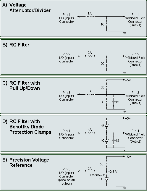
Referring to the figure, let me point out some of the more common options:
- A — Often voltage attenuation may be needed for A/D measurement as shown in Figure 3A. Resistive dividers are produced simply by inserting through-hole resistors at locations nA and nC for circuit n. If you need circuit amplification, then you might take a look at the Signal Conditioning Wildcard.
- B — RC filters are very useful as anti-aliasing filters when using the Analog I/O Wildcard. Figure 3B shows the most simple of these.
- C — Sometimes an input signal should float to an intermediate voltage between power and ground, or it should be shifted as well as attenuated, as shown in the circuit of Figure 3C.
- D — If an input exceeds the voltage levels allowed by your controller or Wildcard, you can clamp the input to the power supply rails using Schottky diodes as show in Figure 3D. For more information about using Schottky diode clamps, see A/D Protection Circuits.
- E — The I/O Filter Wildcard can also serve as a general purpose prototyping board. Figure 3E shows the creation of a 2.5V reference on I/O pin 5 using a precision voltage reference chip and the 5V supply. You can connect IC temperature sensors or thermistors similarly.
Mounting Components on the I/O Filter Wildcard
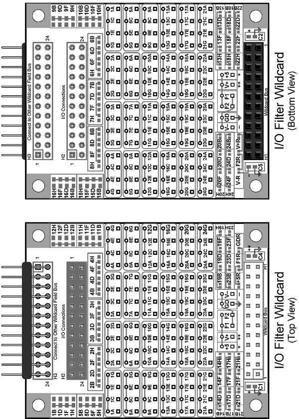
Figure 4 provides a larger-than-life diagram of the top and bottom of the I/O Filter Wildcard so that you can easily see the positions and labels of the components. The board’s silk-screen legend provides the same information, but the print isn’t always legible. You can use Figure 4 as a guide when soldering components to the board.
Through-hole components are mounted in the large central region while surface-mount components are mounted in the peripheral areas. Note that the shapes of the through-hole pads, round or square, correspond to the connection symbols used in Figures 1-3. You should pay attention to these shapes when wiring polarized components.
Surface mount components should use size 0603 packages. They can be mounted on the designated pads. If you use polarized components you'll need to be careful to mount them in the proper direction. You can take your cue for the proper direction from the way the pads are connected together – you'll notice that the pads for one side of each of the four components for each line are all connected together. That side of all the components represents the center node in the circuits of Figure 1.
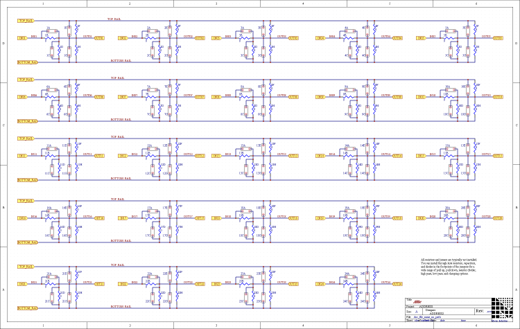
Detailed Hardware Schematics
Size and weight
| Physical Specifications | |
|---|---|
| Weight: | 16 gram |
| Size : | 2" x 2.5" x 0.365"1) (50.8mm x 63.5mm x 9.3mm) |
See also → Modular I/O Boards
