Appendix B: Connector Pinouts
The PDQ Board Starter Kit comprises a stack of two boards: the Docking Panel and the PDQ Board Single Board Computer (SBC). Pin-outs for all input-output (IO) connectors on the PDQ Board and the PowerDock are provided here. You may find PDQ Board physical dimensions here.
PDQ Board connectors
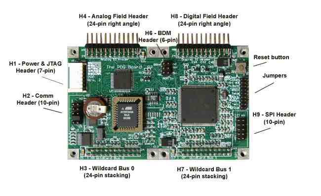
The pinouts of all of the connectors on the PDQ Board are presented below. To locate the connectors on the board, consult Figure B-1 and the white silk–screened labels on the PDQ Board. The arrows in the figure point to the locations of pin 1 on each connector. The large chip on the right side of the board is the Freescale 9S12 (HCS12) microcontroller.
 Figure B-1 Headers and Jumpers on the PDQ Board.
Jumpers
| Jumper | Label | Description |
|---|---|---|
| J1 | Clean | Puts the PDQ Board into special cleanup mode on the next power-up or reset. To return the PDQ Board to its pristine, right-from-the-factory condition, install this jumper, press the Reset Button, and then remove the jumper. |
| J2 | SPI #2 | If installed, configures the board as the bus slave on SPI1, bus master on SPI2. Normally the board is bus master on SPI1 and bus slave on SPI2. |
| J3 | NoBoot | If installed, disables the processing of Boot Vectors. Typically not installed. |
| J4 | 1 485En | If installed, enables RS485, disables RS232 on the Serial1 port |
| J5 | 1 Term | If installed with J4, provides RC termination for the RS-485 communications link on Serial 1 by connecting a 120 Ohm resistor in series with a 0.1 micro-Farad capacitor across the RS485 line. |
| J6 | 1 RTrm | If installed with J4 and J5, shorts out the capacitive termination on RS485-1 serial port, resulting in purely Resistive termination. |
| J7 | 2 485En | If installed, enables RS485, disables RS232 on the Serial2 port |
| J8 | 2 Term | If installed with J7, provides RC termination for the RS-485 communications link on Serial 2 by connecting a 120 Ohm resistor in series with a 0.1 micro-Farad capacitor across the RS485-2 line. |
| J9 | 2 RTrm | If installed with J7 and J8, shorts out the capacitive termination on RS485-2 serial port, leaving the Resistive termination intact. |
Power header
| H1: Power Header | |
|---|---|
| Pin | Signal |
| 1 — | V+RAW (+8 to +26 VDC) |
| 2 — | GND |
| 3 — | +5 VDC |
| 4 — | TDI for JTAG programming |
| 5 — | TMS for JTAG programming |
| 6 — | TCK for JTAG programming |
| 7 — | TDO for JTAG programming |
| Note: V+RAW is needed only if certain Wildcards are used. Pins 4-7 are generally not used. They are used only for Mosaic factory programming of an onboard CPLD. | |
Communications header hosts Serial1 and Serial2 ports
| H2: Communications Header | |||
|---|---|---|---|
| Signal | Pins | Signal | |
| /TxD1 | —1 | 2— | /RxD1 |
| DGND | —3 | 4— | RS485 XCV2+ |
| RS485 XCV1- | —5 | 6— | RS485 XCV1+ |
| /TxD2 | —7 | 8— | /RxD2 |
| DGND | —9 | 10— | RS485 XCV2- |
| H5: Docking Panel Comm Header | |||
|---|---|---|---|
| Signal | Pins | Signal | |
| /TxD1 | —1 | 2— | /RxD1 |
| DGND | —3 | 4— | /MOD1_CS/NC |
| RS485 XCV1- | —5 | 6— | RS485 XCV1+ |
| /TxD2 | —7 | 8— | /RxD2 |
| DGND | —9 | 10— | VBAT |
| Note: This pinout matches the comm socket of the Docking Panel itself, but differs from the comm header (right-angle pins) on the Docking Panel: on the Docking Panel comm header pin 4 is connected to DGND and pin 10 is connected to +5V. Note: This header is actually labeled "PowerDock Hdr" | |||
SPI header hosts SPI1 and SPI2 ports
| H9: SPI Header | |||
|---|---|---|---|
| Signal | Pins | Signal | |
| /SS1 | —1 | 2— | /SS2 |
| SCK1 | —3 | 4— | SCK2 |
| MOSI1 | —5 | 6— | MOSI2 |
| MISO1 | —7 | 8— | MISO2 |
| DGND | —9 | 10— | /XIRQ |
Digital field header
|
Analog field header | ||||||||||||||||||||||||||||||||||||||||||||||||||||||||||||
Wildcard I/O expansion interface
| H3 & H7: Wildcard Port0 & Port1 Headers | |||
|---|---|---|---|
| Signal | Pins | Signal | |
| GND | —1 | 2— | +5V |
| /IRQ | —3 | 4— | V+RAW |
| SEL1/XMIT- | —5 | 6— | SEL0/XMIT+ |
| MOSI/XCV- | —7 | 8— | MISO/XCV+ |
| /RESET | —9 | 10— | SCK |
| /MOD.CS | —11 | 12— | 16MHz |
| E | —13 | 14— | R/W |
| /OE | —15 | 16— | /WE |
| AD7 | —17 | 18— | AD6 |
| AD5 | —19 | 20— | AD4 |
| AD3 | —21 | 22— | AD2 |
| AD1 | —23 | 24— | AD0 |
BDM header
Docking panel connectors
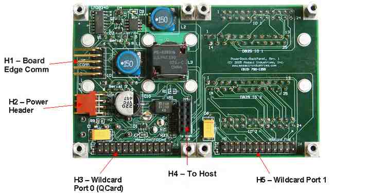
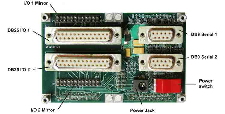
The pin-outs of all of the connectors on the Docking Panel are presented below. To locate the connectors on the board, consult Figure B-2 and the white silk–screened labels on the PowerDock.
H2: Power header
The following table provides the power header’s pinout:
| Power Header | ||
|---|---|---|
| Pin | Signal | |
| 1 | – | VIN (8 to 26 Volts) |
| 2 | – | GND |
| 3 | – | +5 VDC |
| 4 | – | VBAT |
Communications connectors
Standard DB-9 serial connector configurations
|
| ||||||||||||||||||||||||||||||||||||||||||||||||||||||||||||||||||||||||||||||||||||||||||||||||
Standard DB-25 IO headers
|
| ||||||||||||||||||||||||||||||||||||||||||||||||||||||||||||||||||||||||||||||||||||||||||||||||||||||||||||
Communications header
| Docking Panel Communications Header H1 | |||
|---|---|---|---|
| Signal | Pins | Signal | |
| /TxD1 | —1 | 2— | /RxD1 |
| GND | —3 | 4— | GND |
| RS485 XCVR- | —5 | 6— | RS485 XCVR+ |
| /TxD2 | —7 | 8— | /RxD2 |
| GND | —9 | 10— | +5V |
| Note: This pinout differs from that of the PDQ Board pinout; on the PDQ Board pin 4 is connected to XCV2+ and pin 10 is connected to XCV2-. | |||
Wildcard headers H3, H7
| Wildcard Port Header | |||
|---|---|---|---|
| Signal | Pins | Signal | |
| GND | —1 | 2— | +5V |
| /IRQ | —3 | 4— | V+RAW |
| SEL1/XMIT- | —5 | 6— | SEL0/XMIT+ |
| MOSI/XCV- | —7 | 8— | MISO/XCV+ |
| /RESET | —9 | 10— | SCK |
| /MOD.CS | —11 | 12— | 16MHz |
| E | —13 | 14— | R/W |
| /OE | —15 | 16— | /WE |
| AD7 | —17 | 18— | AD6 |
| AD5 | —19 | 20— | AD4 |
| AD3 | —21 | 22— | AD2 |
| AD1 | —23 | 24— | AD0 |
See also → Getting to Know Your Hardware
Using Your Docking Panel


