Simulating Open Collector Outputs
Convert totem pole microcontroller digital outputs to open collector behavior
When driving external devices, it is sometimes necessary to use open-collector or open-drain outputs. Open-collector or open-drain outputs do not source current, they can only sink current. Essentially, they act as simple switches to ground. In their high state, they are open circuits, and in their low state they pull the output pin to ground, sinking as much current as needed, up to a limit.
The digital outputs of the PDQ Board, QCard Controller, and other Wildcards are not open-collector. Instead, they are more generally useful totem-pole, three-state outputs — they have transistors to actively source current for a logic high, and to sink current for logic low, as well as the ability to turn off both transistors to isolate the output in a high impedance state. When in the high impedance state the pins can usually be used as inputs. But sometimes your application may require the simpler open collector output. For example, to drive 3.3 volt logic devices you would not want to drive their inputs to a 5 volt logic high, as it would be greater than their power supply voltage. So, you would use an open collector output to actively drive the external input low, but allow it to be pulled high passively by a pull-up resistor only to 3.3V.
There are two ways to make a PDQ Board output pin simulate the behavior of an open-collector pin, one in software and one in hardware. In either case, you can use the output to connect to devices that pull-up to a voltage less than 5V, such as 3.3V logic inputs. You can not connect use these methods to connect to external voltages greater than 5V, as that may harm the output pin.
Software simulation of an open collector output
You can make an output pin behave like an open collector output (within the constraint that no more than 5V is applied to it) by only driving it into two of its possible states: high impedance input and active low output.
While a digital I/O pin is configured as an input you can set it to a low state, then you can enable it as an output. The output switches from its high impedance state to an active low, just as an open collector output would do. To turn it off, merely reconfigure it as an input.
For example, on the PDQ Board, to use to a PORTM pin as an open collector output, you would first configure the pin as an input by writing a 0 to the corresponding bit position in PORTM_DIRECTION. Then write a 0 to the pin by writing to the appropriate bit of PORTM. The output will remain in its high impedance state, pulled high by the external device. Turn the output ON, making the pin active low, by reconfiguring it as an output by writing a 1 to the corresponding bit position in PORTM_DIRECTION. You can then turn it back OFF by reconfiguring it as an input by writing a 0 back to PORTM_DIRECTION. You can find more detailed instructions for configuring the digital I/O pins in the Digital I/O section of the PDQ Board Users Guide.
Failsafe hardware open collector outputs
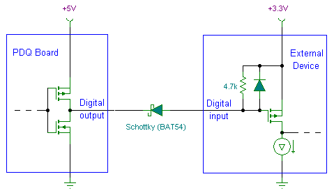
A hardware modification can provide a more fault-tolerant solution. When using a strictly software approach, if by some software error the pin is set to output a high level, then a low voltage external device could be harmed. That fault can be prevented by placing a Schottky diode in series with the digital output pin. It's a failsafe way of forcing a digital output to appear as an open-collector output. That way, if the digital output were to be inadvertently set high, the Schottky diode would prevent any current flow. When the pin is set low, the Schottky diode conducts. Here's a circuit schematic of a typical application, in which the digital output drives an external device that expects to be driven by an open collector output:

You can use any low cost, low voltage Schottky diode – the popular BAT54 is shown in the schematic. The output pin uses an internal MOSFET transistor, so it can pull fully down to ground. When the output is low, the Schottky diode will add a little offset voltage of only about 200 millivolts. That is still low enough to be interpreted by the external device as a valid logic low level. In this case the pull-up resistor, which pulls up the output to 3.3V when it is not driven low, is built into the external device. In other applications you may need to provide an separate pull-up resistor to an appropriate voltage.
You can use these methods to allow a 5V logic level output to safely drive a lower voltage external input. However, even with these methods you should not connect the 5V output to external voltages greater than 5V, as that may harm the output pin.
External media: TINA-TI schematic
