Using High Frequency PWM
Output rise and fall times and turn ON/OFF delays determine the maximum frequency of PWM current waveforms
The PWM Driver Wildcard is used in conjunction with the PDQ Board line of products to convert their 9S12/HCS12 MCU-generated PWM outputs into the high currents and voltages required of motors, valves, heaters and other high current devices. Devices can be turned on and off at low frequencies without regard to the dynamic performance of the PWM Driver Wildcard, but operating it at high frequency requires understanding its turn on/off times and slew rates.
The PWM outputs of the PWM Driver Wildcard do not switch instantaneously, but require a little time to turn ON and OFF. The 9S12 HCS12 MCU PWM outputs are very fast, but by design the Wildcard's outputs are slew-rate-limited to minimize the radiation and propagation of switching noise.1) Combined, turn on/off delays and finite slew rates place a limit the maximum frequency of operation, as well as the accuracy of the duty cycle produced.
The PWM Driver Wildcard will function at frequencies as great as 2 MHz, but there is not much dynamic range in the duty cycle produced at such high frequency. More realistically, you can pulse width modulate high currents accurately and efficiently at frequencies as great as 100 KHz. At that frequency the duty cycle error grows to about 1%. (It is proportional to frequency, at 10 KHz it is less than 0.1%.)
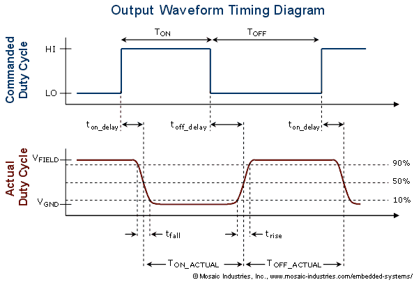
To understand the determinants of the maximum frequency we'll consider the turn ON/OFF delays and slew rates as defined in the following timing diagram, Figure 1, which shows a full cycle of the output waveform.

In the figure the top trace represents the voltage applied to the gate of the low-side MOSFET driver, while the lower trace represents the voltage present at the MOSFET's drain, the OUT- output line of the PWM Driver Wilcard. The MOSFET inverts the voltage, so when it is ON it converts the high input voltage to a low output voltage.
There are slight delays between the commanded output and the change in output voltage, measured to the 50% voltage threshold. Because the ON and OFF transition delays are not perfectly balanced, there is a net lengthening of the ON time portion of the waveform (i.e., it takes longer to turn OFF the pulse than to turn it ON). The values of rise and fall times, and ON time lengthening were carefully measured and found to be those of the following table.
| Parameter | Time | Notes |
|---|---|---|
| Turn ON time: | <0.12 μsec | For an output voltage fall from 90% to 10%. |
| Turn OFF time: | <0.2 μsec | For an output voltage rise time from 10% to 90%. |
| ON time lengthening: | 0.12 μsec | Measured at the 50% level of the rising and falling transitions. |
Because the ON and OFF rise/fall times are not balanced there is a net gain in ON time – an ON pulse is effectively lengthened by 0.12 microsecond for pulse ON times greater than 0.2 μsec. The minimum usable ON and OFF times are approximately 0.2 and 0.3 μsec respectively.
The pulse lengthening causes a negligible duty cycle error at low PWM frequencies, but increases linearly with frequency becoming an approximately 1.2% error at 100 kHz.
About the measuring ON/OFF times of open-drain MOSFETs
If you are driving resistive loads the output waveform should look like a clean square wave as you increase frequency. But if the load is inductive or capacitive then the waveform may be a bit different, and frequency dependent. If the resistance is great, then the capacitance of the output will dominate the waveform and you will only see a slow voltage ramp when the channel is turned OFF.
Because the output is active low, whatever kind of load is connected, so long as the current is not too great, when the output is ON the voltage at the OUT- pins will be low. The voltage is actively pulled down by the MOSFET output stage, so the low portion of the output voltage waveform will always look clean, and the turn ON time can be measured easily.
But when the output turns OFF the output is not actively pulled high; instead, it is pulled to the supply voltage by the load. Consequently, the transition from a low output voltage to a high output voltage will be dominated by the dynamics of the load. Generally, for inductive loads, the voltage will climb higher than the field supply voltage, turning on the flyback protection diodes on the board until the inductor current decays. Then you may see an oscillation around the field supply voltage with a frequency determined by the load inductance and capacitance. If you are driving a motor, you will see the speed-dependent back EMF produced by the motor.
For low currents (<10 mA for example) into a high inductance, you may see that the output voltage rise time is slowed as the turning off MOSFETs are able to sink the inductor's current and the L/R time constant is appreciable. What looks like a slow turn-OFF does not cause a duty cycle error, as the current that is flowing is the inductor decay current, which will flow whatever the apparent OFF voltage trajectory. For greater currents the turning OFF MOSFETs can't support the inductor current and the inductor forces the voltage to fly up to more than the supply voltage quickly.
For capacitive loads or high resistance loads, the output capacitance will charge linearly through the load resistance toward the supply voltage.
