Appendix B: Connector Pinouts
The QVGA Controller comprises a stack of three boards: a display backplane, the QVGA Board, and the smaller QED-4-QVGA Board (aka QED-Flash Board). Pin-outs for all I/O connectors on the QED-Flash Board or the QVGA Board are provided here.
Warning – Do Not Connect to System Control Signals
When connecting to the Digital I/O Connector (H2 on the QVGA Board) with a ribbon cable, notch out cable wires 11 through 24. Even short pieces of wire connected to some of these lines may cause intermittent operation of the touchscreen or processor.
When connecting to the Supplemental I/O Connector (H3 on the QED Board) with a ribbon cable, only connect the wires you need, and do not connect to the data bus lines or system control lines.
QED Flash Board Connectors
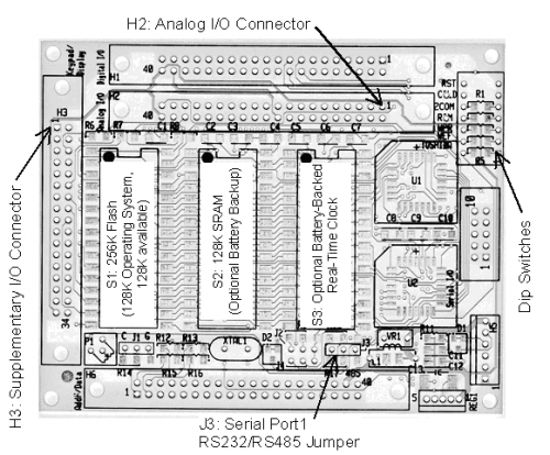
The pinouts of all of the connectors on the QED–Flash Board are presented below. To locate the connectors on the board, consult Figure B–1 and the white silk–screened labels on the visible side of the QED–Flash Board. The arrows in the figure point to the locations of pin 1 on each connector.

QED–Flash Board Connectors and Switches. Arrows locate pin 1 of each connector.
| H3: Supplemental I/O Connector |
|---|
| | | Signal | Pins | Signal |
|---|
| PPB4 | – 1 | 2 – | GND | | PPB3 | – 3 | 4 – | +5V | | PPC3 | – 5 | 6 – | Vcontrast | | PPC0 | – 7 | 8 – | A1 | | PPB2 | – 9 | 10 – | R//W | | PPC1 | – 11 | 12 – | Display.E | | PPC2 | – 13 | 14 – | D0 | | PPB1 | – 15 | 16 – | D1 | | PPB0 | – 17 | 18 – | D2 | | DGND | – 19 | 20 – | D3 | | HC0* | – 21 | 22 – | D4 | | HC1 (PB5)* | – 23 | 24 – | D5 | | HC2 (PB6)* | – 25 | 26 – | D6 | | HC3 (PB7)* | – 27 | 28 – | D7 | | DGND | – 29 | 30 – | DGND | | SNUB | – 31 | 32 – | +5VDD | | V+RAW | – 33 | 34 – | VEE | * HC0 is generated by the PAL, HC1–HC3 are generated from PB5–PB7 respectively.
You should not connect to the grayed-out signals. Even a short wire connected to these lines may cause malfunction. | |
| H6: Address/Data |
|---|
| | | Signal | Pins | Signal |
|---|
| PG7 | – 1 | 2 – | PG6 | | PG5 | – 3 | 4 – | PG4 | | PG3 | – 5 | 6 – | PG2 | | PG1 | – 7 | 8 – | PG0 | | A15 | – 9 | 10 – | A14 | | A13 | – 11 | 12 – | A12 | | A11 | – 13 | 14 – | A10 | | A9 | – 15 | 16 – | A8 | | A7 | – 17 | 18 – | A6 | | A5 | – 19 | 20 – | A4 | | A3 | – 21 | 22 – | A2 | | A1 | – 23 | 24 – | A0 | | D7 | – 25 | 26 – | D6 | | D5 | – 27 | 28 – | D4 | | D3 | – 29 | 30 – | D2 | | D1 | – 31 | 32 – | D0 | | /RESET | – 33 | 34 – | R//W | | /OE | – 35 | 36 – | /WE | | E | – 37 | 38 – | V+Raw | | DGND | – 39 | 40 – | +5V | | You should not generally need to connect to the processor's address and data bus. Please consult Mosaic Industries before attempting to connect to these signals. |
| H2: Analog I/O Connector |
|---|
| | | Signal | Pins | Signal |
|---|
| Vrl | – 1 | 2 – | Vrh | | PE7/AN7 | – 3 | 4 – | PE6/AN6 | | PE5/AN5 | – 5 | 6 – | PE4/AN4 | | PE3/AN3 | – 7 | 8 – | PE2/AN2 | | PE1/AN1 | – 9 | 10 – | PE0/AN0 | | 12AN7 | – 11 | 12 – | 12AN6 | | 12AN5 | – 13 | 14 – | 12AN4 | | 12AN3 | – 15 | 16 – | 12AN2 | | 12AN1 | – 17 | 18 – | 12AN0 | | AGND | – 19 | 20 – | +5VAN | | Vin1 | – 21 | 22 – | Vout1 | | Vin2 | – 23 | 24 – | Vout2 | | Vin3 | – 25 | 26 – | Vout3 | | Vin4 | – 27 | 28 – | Vout4 | | Vin5 | – 29 | 30 – | Vout5 | | Vin6 | – 31 | 32 – | Vout6 | | Vin7 | – 33 | 34 – | Vout7 | | Vin8 | – 35 | 36 – | Vout8 | | 1.5Vref | – 37 | 38 – | +5V | | Analog Bus V– | –39 | 40 – | V+Raw | | Processor Port E may be used as either 8–bit A/D inputs (AN0–7) or as digital inputs. 12AN0-7 are 12-bit A/D inputs. Vin1-8 and Vout1-8 are the 8-bit multiplying DAC inputs and outputs. | |
QVGA Board Connectors
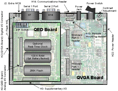
The pin-outs of all of the connectors on the QVGA Board are presented below. To locate the connectors on the board, consult Figure B-2 and the white silk–screened labels on the visible side of the QVGA Board.

Connectors and Switches on the QVGA Controller
| H22: Power Header |
|---|
| | | Signal | Pins | Signal |
|---|
| GND | – 1 | 2 – | GND | | V+Raw | – 3 | 4 – | V+Bias | | +12 V / +5 V ALT | – 5 | 6 – | +5 V | | +5 VAN | – 7 | 8 – | +3.3 V | | MONO_VEE | – 9 | 10 – | GND |
| Serial 1 Connector |
|---|
| | | Signal | Pins | Signal |
|---|
| NC | – 1 | | | | | | 6 – | DSR1/DTR1 | | TXD1 | – 2 | | | | | | 7 – | CTS1 | | RXD1 | – 3 | | | | | | 8 – | RTS1 | | DSR1/DTR1 | – 4 | | | | | | 9 – | NC | | DGND | – 5 | | | | Notes: | | NC indicates no connection | | Pins 4 and 6 (DSR1/DTR1) are connected. | | Pins 7 and 8 (CTS1/RTS1) may optionally be connected on the board with zero ohm shorts. |
| Serial 2 Connector |
|---|
| | | Signal | Pins | Signal |
|---|
| NC | – 1 | | | | | | 6 – | DSR2/DTR2 | | TXD2 | – 2 | | | | | | 7 – | CTS2/RTS2 | | RXD2 | – 3 | | | | | | 8 – | RTS2/CTS2 | | DSR2/DTR2 | – 4 | | | | | | 9 – | NC | | DGND | – 5 | | | | Notes: | | NC indicates no connection | | Pins 4 and 6 (DSR2/DTR2) are connected. | | Pins 7 and 8 (CTS2/RTS2) are connected. |
| H14: Serial Communications Connector |
|---|
| | | Signal | Pins | Signal |
|---|
| TxD1 | – 1 | 2 – | RxD1 | | DGND | – 3 | 4 – | DGND | | XCVR- | – 5 | 6 – | XCVR+ | | TxD2 | – 7 | 8 – | RxD2 | | DGND | – 9 | 10 – | DGND |
| Wildcard Port Header |
|---|
| | | Signal | Pins | Signal |
|---|
| GND | – 1 | 2 – | +5V | | /IRQ | – 3 | 4 – | V+Raw | | PG1/XMIT- | – 5 | 6 – | PG0/XMIT+ | | MOSI/XCV- | – 7 | 8 – | MISO/XCV+ | | /RESET | – 9 | 10 – | SCK | | /MOD.CS | – 11 | 12– | 16 MHz | | E | – 13 | 14 – | R/W | | /OE | – 15 | 16 – | /WE | | AD7 | – 17 | 18 – | AD6 | | AD5 | – 19 | 20 – | AD4 | | AD3 | – 21 | 22 – | AD2 | | AD1 | – 23 | 24 – | AD0 |
| H2, H4: Digital I/O Connector | |
|---|
| | | | Signal | Pins | Signal | |
|---|
| GND | – 1 | 2 – | +5V | | | PA7 | – 3 | 4 – | PA6 | | | PA5 | – 5 | 6 – | PA4 | | | PA3 | – 7 | 8 – | PA2 | | | PA1 | – 9 | 10 – | PA0 | | | PD5//SS | – 11 | 12 – | PD4/SCK | | | PD3/MOSI | – 13 | 14 – | PD2/MISO | | | E | – 15 | 16 – | R//W | | | /OE | – 17 | 18 – | /WE | | | /XIRQ | – 19 | 20 – | /IRQ | | | PFI Input | – 21 | 22 – | 4xOut | | | /Reset | – 23 | 24 – | /Shutdown | | | PPC7 | – 25 | 26 – | PPC6 | | | PPC5 | – 27 | 28 – | PPC4/RS485.XMIT | | | PPA7 | – 29 | 30 – | PPA6 | | | PPA5 | – 31 | 32 – | PPA4 | | | PPA3 | – 33 | 34 – | PPA2 | | | PPA1 | – 35 | 36 – | PPA0 | | | AGND | – 37 | 38 – | +5VAN | | | DGND | – 39 | 40 – | V+Raw | | | Notes: | | Headers H2 and H4 are connected in parallel. H4 connects to the QED Board, and H2 is available for you to connect to. | | | You should not need to connect to the grayed-out signals. When connecting a ribbon cable to H2 you should notch out the wires corresponding to the shaded signals, pins 11 through 24. Even short lengths of wire connected to these signals may cause intermittent operation of the processor or the touchscreen. | | |
This page is about: 68HC11 MUC QVGA Controller Connector Pinouts for Analog and Digital I/O – The QVGA Controller comprises stack of three boards: display backplane, QVGA Board, and smaller QED 4 QVGA Board (aka QED Flash Board). Pin outs for all I/O connectors on QED Flash Board or QVGA Board are provided here. Warning - Do Not Connect to System …


