Latch and Toggle Power Circuits
MOSFET transistor circuits power an embedded system ON and OFF with the push of a button.
This page provides soft power switch circuits for toggling electronic devices ON and OFF with a momentary button press that controls a latching high-side MOSFET power switch. Several micropower latching switch circuits are provided. Owing to their low current in the OFF state, they're well suited to battery operated portable instruments. Feel free to use these circuits as is, or modify them for your needs, wherever you might need a power bus switch circuit.
Depending on your application, you may need one of two ON/OFF behaviors:
- Press-ON-Press-OFF soft toggle action, where a short button press of a tactile switch latches the circuit ON and another toggles it back OFF; or,
- A Press-ON-Hold-OFF action, where a short press turns power to a circuit ON, but a longer button hold is needed to toggle it OFF.
The soft power switch circuit designs shown on this page provide both functions. You may also be interested in:
- ON/OFF switches that limit capacitor in-rush currents, or,
- switches to specifically turn ON/OFF microcontroller products.
Press ON - Press OFF soft latching circuits
Using a single tactile switch button to alternately toggle a circuit ON and OFF requires a circuit containing a bistable logic latch. Such a latch can be implemented using a D flop flop, or by using positive feedback around any two inverting amplifiers or logic gates. For example, a basic latching ON-OFF switch can be implemented using a dual NAND gate, using this circuit:
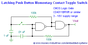
A brief button press toggles the output state of this NAND gate latch. Any CMOS NAND gate can be used, including Schmitt trigger gates. In fact, any inverting devices can be used with minor changes to the circuit: a hex inverter, open collector inverters, NAND or NOR gates, transistors, FETs or MOSFETs.
When power is first applied, the capacitor at the input of the first gate guarantees that the latch output, Vout, is initially latched low. Thereafter, button presses toggle the output high and low.
To turn the latch into a power switch, the NAND gate output may be used to control a P-MOSFET high-side switch, as shown here:
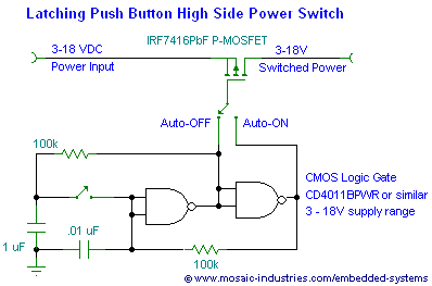
The IFR7416 MOSFET shown tolerates a maximum gate-source voltage of 20V, and the CD4011 withstands up to 20V, but is rated for 18V max operation.
The high-side switch can do double duty as one of the two active devices needed to form the latch, as shown in the following two MOSFET circuits:
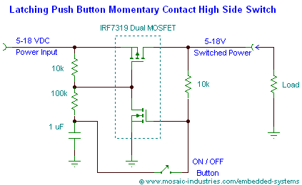
This circuit uses only a single active device, the surface mount dual MOSFET, yet toggles ON and OFF currents of up to 4 Amp. The load may be just about any electrical device, from high power LED lights to the power supply of embedded computers.
Driving capacitive loads
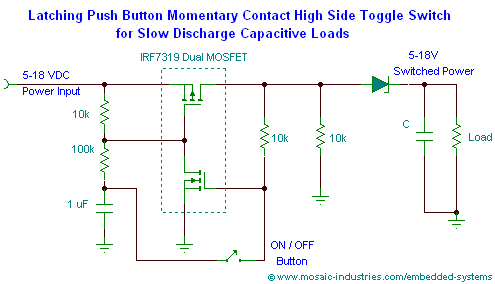
Placing the high side MOSFET switch within the feedback path for the latch does introduce a potential failure if the output drives slow-decay capacitive loads, as it might in power bus switches. If the switch applies power to a power supply with large input capacitors, and the load does not draw enough current for those capacitors to discharge quickly, then the transient button press may not turn OFF the switch reliably. Instead, after the high-side switch turns OFF, the sustained voltage at its output, propped up by the large capacitors, keeps the lower MOSFET turned ON, which in turn activates the high side switch after the button release.
One way of preventing that failure mode is to place a Schottky diode in series with the load, as shown in this circuit schematic:
Press ON - Hold OFF latching circuits
For controlling smart products containing microcontrollers you often want to ensure that the power is not inadvertently removed. Consequently, you want a power switch that can be turned ON by a brief button press, but requires a longer, deliberate button hold to turn it OFF. That prevents accidentally killing power if the tactile switch is unintentionally touched.
The following shows a NAND gate latch implementing the desired action:
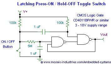
When power is first applied, the output is held low for 3 seconds, during which time the button has no effect. After that, a momentary press latches the output high, and a long press of greater than 3 seconds latches the output low again. You can use the output to turn ON and OFF a variety of devices, including MOSFET hogh- or low-side switches. The output of the other NAND gate can be used if an inverted logic level is needed.
The following schematic shows a very useful circuit for controlling a high side switch (a P-MOSFET) similarly. The circuit uses only one active component, a dual MOSFET, which provides the latching logic and acts as a high side power switch/relay. A momentary button press causes the circuit to latch ON, supplying power to the load, and it is turned back OFF by a longer button hold. It can supply power of 5 to 18 volts at up to 4 amps.
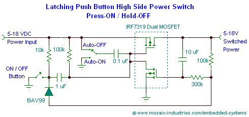
In the initial OFF state, this circuit uses no power – the only current drawn is the sub-microamp reverse leakage currents of the diode and the MOSFETs. Even in the ON state the circuit draws very little bias current to maintain its latched state – only the series pass transistor dissipates some power as it passes the load current. And that power is minimal; the P-MOSFET has an ON resistance of only 58 milli-Ω.
When in its OFF state, momentarily pressing the tactile button turns ON the switched power and it latches ON, supplying power to the output. While it is ON, pressing and holding the button for more than 3 seconds turns the power switch back OFF, and it stays OFF until the next momentary button press. For it to reliably turn OFF, the load should draw sufficient current so that any downstream capacitors will discharge within a few seconds, allowing the gate drive of the N-MOSFET to decay.
The RDS-ON of the P-MOSFET used as the high-side switch is only 0.058 ohms so its small surface mount package doesn't heat much, even at currents of 4 amp. The input voltage is limited by the maximum gate-source voltage, VGS, of the MOSFETs, which is 20V – so I recommend a maximum input voltage of 18V, allowing a safety margin of 2V.
Both N-type and P-type MOSFETs are provided in a single SMD package as part number IRF73191), making the circuit's total real estate requirement minimal. The package includes ultra-low ON resistance N- and P-MOSFETs. As it's quite a versatile device, for your convenience you can view or download the IRF7319 datasheet here:
The 10μF capacitor should be a low leakage variety – a ceramic capacitor works well.
Circuit operation is as follows: When power is first applied, the source-gate voltage of the P-FET either remains zero, keeping the high side switch OFF, or the gate is held low as the source rises, turning on the MOSFET, depending on the position of the Auto-ON jumper. When the MOSFET is OFF, a momentary touch of the ON/OFF button pulls the gate low for tens of milliseconds, fully turning on the high side MOSFET. The output voltage rise is transmitted to the N-MOSFET's gate through the 10μF capacitor and resistors, turning it ON. With the low-side FET ON, the gate of the high-side FET is pulled low, keeping it turned ON. Consequently, the power latches ON even after the button is released. Only a few volts of VGS is sufficient to keep the MOSFETs turned fully ON.
Subsequently, a long button touch turns the circuit OFF. Pressing and holding the button down pulls down the gate of the low-side MOSFET after a few second delay determined by the discharge of the 10μF capacitor through the 300 kΩ resistor. The low-side MOSFET turns OFF, allowing the gate of the high-side MOSFET to rise to its source voltage, turning it OFF too. So long as the load voltage drops within a second or so (that is, it is not held up by any really big output capacitors), the power latches OFF until the next momentary press of the ON/OFF button.
The feedback capacitor allows operation even with moderate capacitive loads (slowly decaying output voltage). The user holds the button until noticing that the power is switched OFF. At that time the load is decaying, and the -dV/dt of the output voltage is transmitted by the feedback capacitor to the gate of the N-MOSFET, holding it OFF even when the output voltage is still above the MOSFET's turn on voltage.
Controlling power ON startup behavior
You can control the start-up behavior of the circuit so that it either turns ON automatically when power is first applied or remains OFF. In the following circuit, if the Auto-ON jumper connects the 0.1μF capacitor to ground (or if it is permanently wired that way) then the circuit turns ON if power is applied to its input suddenly. In the other position (or if the 0.1μF capacitor is wired permanently to the input power rail), the circuit remains in its OFF state when power is applied.

The circuit operates up to 18V input – in no case should you risk a voltage as great as 20V, as that is the minimum breakdown gate-source breakdown voltage of the MOSFETs. See the following section – Using high-side MOSFET switches at higher voltages – for guidance on controlling higher voltages.
The following schematic shows a similar circuit, but one which also provides a controlled slew rate for its output voltage for downstream in-rush current limiting:
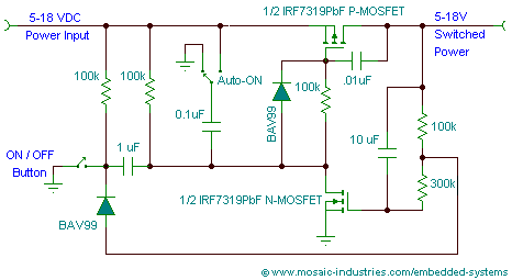
To learn more about in-rush current limiting for high-side switches, see Limiting In-rush Current in MOSFET Power Switches.
Using high-side MOSFET switches at higher voltages
While many MOSFETs can be used to switch high voltages – that is, a high voltage across their drain-source terminals – they can not tolerate too great a source-gate voltage. Usually the source-gate voltage causes break down at 12 to 20V. One limitation of the above circuits is that the input voltage range is limited to less than 20V by the maximum allowed VGS of the IRF7319 MOSFET transistors.
To use the MOSFET with a higher voltage supply requires that we protect the gate-source junction, as shown in the following circuit which uses a Zener diode to protect the MOSFET gate:
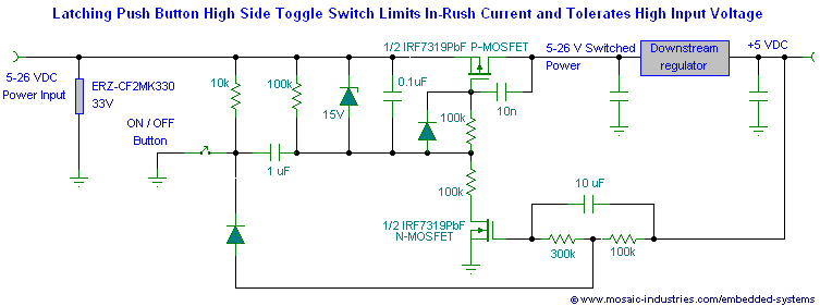
Here a 15V Zener diode limits the voltage across the gate-source junction. When the N-MOSFET turns ON, it pulls the gate of the high-side switch, the P-MOSFET, towards ground, turning it ON too. The P-MOSFET's gate voltage is prevented from going more than 15V below its source voltage by the Zener diode clamp. The N-MOSFET's gate is driven by the output of a lower voltage regulator, so it doesn't require similar protection.
The addition of the 15 volt Zener allows extends the input voltage range to the VDS_MAX of the MOSFETS, which for the IRF7319 is 30V. The input is specified at a maximum of 26V, to allow some safety margin. A somewhat higher voltage MOSFET pair that may be used is the FDS4897C, rated at 40V.
A transient protection device, the 33V varistor2), is also included. It is fully turned OFF at 26V, but starts turning ON at greater voltages, and sinks lots of current at 33V.
The circuit is shown powering a downstream regulator whose output provides the feedback voltage to the low-side MOSFET. If instead the feedback voltage were to be taken directly from the output of the high-side MOSFET, as is done in the circuits shown earlier, then the gate of the low-side transistor should also be protected. It could be protected by simply tying another 15V Zener directly from its gate to ground.
In this circuit, as in the others, so that the circuit can turn OFF, the capacitors downsteam of the high side switch should not be so great as to hold up the gate of the N-MOSFET for very long after the P-MOSFET switches OFF.
Using high-side MOSFET switches at low (battery) voltages
To use the circuits on this page at low voltages, as provided by one or two AAA or AA battery cells in series, you'll need MOSFETs with low gate threshold voltages. You'll find appropriate MOSFET selection and circuits at:
To learn more about using MOSFETs as power switches, consult these very good application notes and data sheets:
Schematic files: TINA-TI Schematic file
