Appendix A - QED Connector Pinouts
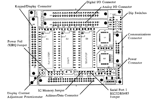
The pinouts of all of the connectors on the QED Board are presented below. To locate the connectors on the board, consult Figure A.1 and the white silkscreened labels on the "memory side" of the QED Board. On the "processor side" of the board, the legend indicates the location of pin 1 and the highest numbered pin on each connector.
Note that some signals have compound names to suggest multiple functions. For example, PPC4/RS485.XMIT on the digital I/O bus is a signal that can be configured as a general purpose digital I/O line named PPC4, or as a signal that controls the direction of data flow if the RS485 serial port is in use. Also note that pins labeled "N/C" are not connected to anything.

Figure A.1 Diagram of the memory side of the QED Board with each of the key components and connectors labeled.
| QED Communications Connector |
|---|
| TxD1 | - 1 | 2 - | RxD1 |
| DGND | - 3 | 4 - | DGND |
| XCVR- | - 5 | 6 - | XCVR+ |
| TxD2 | - 7 | 8 - | RxD2 |
| DGND | - 9 | 10 - | DGND |
| QED Power Connector |
|---|
| /Shutdown | - 1 |
| AGND | - 2 |
| +5VAN | - 3 |
| DGND | - 4 |
| +5V | - 5 |
| 6-12VDC Raw Vin | - 6 |
| Address/Data Connector |
|---|
| PG7 | - 1 | 2 - | PG6 |
| PG5 | - 3 | 4 - | PG4 |
| PG3 | - 5 | 6 - | PG2 |
| PG1 | - 7 | 8 - | PG0 |
| A15 | - 9 | 10 - | A14 |
| A13 | - 11 | 12 - | A12 |
| A11 | - 13 | 14 - | A10 |
| A9 | - 15 | 16 - | A8 |
| A7 | - 17 | 18 - | A6 |
| A5 | - 19 | 20 - | A4 |
| A3 | - 21 | 22 - | A2 |
| A1 | - 23 | 24 - | A0 |
| D7 | - 25 | 26 - | D6 |
| D5 | - 27 | 28 - | D4 |
| D3 | - 29 | 30 - | D2 |
| D1 | - 31 | 32 - | D0 |
| /RESET | - 33 | 34 - | R//W |
| /OE | - 35 | 36 - | /WE |
| E | - 37 | 38 - | V+Raw |
| DGND | - 39 | 40 - | +5V |
| Keypad/Display Connector |
|---|
| PPB4/KPR4 | - 1 | 2 - | GND |
| PPB3/KPR3 | - 3 | 4 - | +5V |
| PPC3/KPC3 | - 5 | 6 - | Vcontrast |
| PPC0/KPC0 | - 7 | 8 - | PPB5/Display.RS |
| PPB2/KPR2 | - 9 | 10 - | GND |
| PPC1/KPC1 | - 11 | 12 - | PPB6/Display.E |
| PPC2/KPC2 | - 13 | 14 - | GND |
| PPB1/KPR1 | - 15 | 16 - | GND |
| PPB0/KPR0 | - 17 | 18 - | GND |
| N/C | - 19 | 20 - | GND |
| N/C | - 21 | 22 - | PPB0/Display.D4 |
| N/C | - 23 | 24 - | PPB1/Display.D5 |
| N/C | - 25 | 26 - | PPB2/Display.D6 |
| N/C | - 27 | 28 - | PPB3/Display.D7 |
| N/C | - 29 | 30 - | +5V for remote potentiometer |
| N/C | - 31 | 32 - | Vcontrast for remote potentiometer |
| N/C | - 33 | 34 - | GND for remote potentiometer |
| Digital I/O Connector |
|---|
| GND | - 1 | 2 - | +5V |
| PA7 | - 3 | 4 - | PA6 |
| PA5 | - 5 | 6 - | PA4 |
| PA3 | - 7 | 8 - | PA2 |
| PA1 | - 9 | 10 - | PA0 |
| PD5//SS | - 11 | 12 - | PD4/SCK |
| PD3/MOSI | - 13 | 14 - | PD2/MISO |
| E | - 15 | 16 - | R//W |
| /OE | - 17 | 18 - | /WE |
| /XIRQ | - 19 | 20 - | /IRQ |
| /Power Fail | - 21 | 22 - | 4xOut |
| /Reset | - 23 | 24 - | /Shutdown |
| PPC7 | - 25 | 26 - | PPC6 |
| PPC5 | - 27 | 28 - | PPC4/RS485.XMIT |
| PPA7 | - 29 | 30 - | PPA6 |
| PPA5 | - 31 | 32 - | PPA4 |
| PPA3 | - 33 | 34 - | PPA2 |
| PPA1 | - 35 | 36 - | PPA0 |
| AGND | - 37 | 38 - | +5VAN |
| DGND | - 39 | 40 - | V+Raw |
| Analog I/O Connector |
|---|
| Vrl | - 1 | 2 - | Vrh |
| PE7/AN7 | - 3 | 4 - | PE6/AN6 |
| PE5/AN5 | - 5 | 6 - | PE4/AN4 |
| PE3/AN3 | - 7 | 8 - | PE2/AN2 |
| PE1/AN1 | - 9 | 10 - | PE0/AN0 |
| 12AN7 | - 11 | 12 - | 12AN6 |
| 12AN5 | - 13 | 14 - | 12AN4 |
| 12AN3 | - 15 | 16 - | 12AN2 |
| 12AN1 | - 17 | 18 - | 12AN0 |
| AGND | - 19 | 20 - | +5VAN |
| Vin1 | - 21 | 22 - | Vout1 |
| Vin2 | - 23 | 24 - | Vout2 |
| Vin3 | - 25 | 26 - | Vout3 |
| Vin4 | - 27 | 28 - | Vout4 |
| Vin5 | - 29 | 30 - | Vout5 |
| Vin6 | - 31 | 32 - | Vout6 |
| Vin7 | - 33 | 34 - | Vout7 |
| Vin8 | - 35 | 36 - | Vout8 |
| 1.5Vref | - 37 | 38 - | +5V |
| VRefLow | - 39 | 40 - | V+Raw |
This page is about: Microcontroller Connector Pinouts 68HC11 MC68HC11F1 – The pinouts of all of connectors on QED Board are presented below. To locate connectors on board, consult Figure A.1 and white silkscreened labels on memory side of QED Board. On processor side of board, legend indicates location of pin 1 and highest …

