Chapter 13 - Powering the QED Board
Getting Started
A 6 Volt DC transformer is included with your QED Developer Package or QED Product Design Kit so that you can power up your QED Board and get started quickly. If you have a Product Design Kit, simply plug the transformer into a wall outlet and plug the transformer's output jack into the receptacle marked "6-12 VDC" on the back panel of the enclosure. If you have a stand-alone QED Board, connect the power cable to the 6-pin power connector on the QED Board, and plug the transformer's output jack into the receptacle at the end of the power cable. Consult the "Getting Started with the QED Board" booklet for more detailed information.
Onboard Power Conditioning and Regulation
The QED Board includes surge suppression, transient filtering, and low-dropout voltage regulation to provide clean 5 Volt supplies for the onboard analog and digital electronics. The board can be powered by batteries (6 Volts or higher), regulated or unregulated DC power (6 to 12 Volts), or a regulated 5 Volt supply. This section explains the onboard power conditioning and regulation circuitry.
Power Input
The DC power input to the QED Board is typically connected to the "Raw.Vin" pin at the power connector on the QED Board. This power input can be generated by the supplied plug-in wall transformer (also called a "wall adapter"), a 6 Volt or 9 Volt battery pack, or any other regulated or unregulated DC supply between 6 Volts and 12 Volts.
The output of the wall adapter is a poorly regulated "raw" input voltage. The typical output of the "6 Volt DC" wall adapter varies between 7.4 Volts and 8.0 Volts if no additional circuitry is attached to the QED Board. Onboard circuitry conditions and regulates this power source to provide clean voltage supplies for the onboard analog and digital electronics.
Surge Suppression
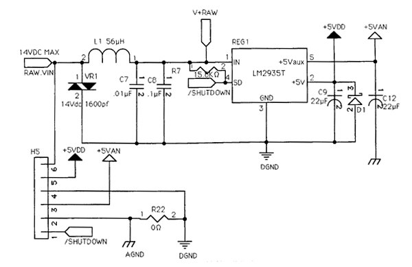
Figure 13.1 is a schematic of the power conditioning and regulation circuitry. The Raw.Vin input is protected by a "varistor" (labeled VR1) rated at 14 Volts DC. This metal oxide device is a surge suppresser. It protects the circuitry on the QED Board by clamping high voltage spikes before they have a chance to do any harm. The varistor has no effect if the input voltage is less than 14 Volts. Above 14 Volts, however, the device starts to conduct current, and it acts like a short circuit to high voltages, thus clamping the voltage spikes. Note that DC voltages in excess of 14 Volts will cause the varistor to continuously conduct current. For this reason you should make sure that the maximum DC voltage supplied to the board is less than 14 Volts; the recommended input range is 6 to 12 Volts.
Figure 13.1 Schematic of the onboard power conditioning and regulation circuitry.
EMI Filter
Additional protection is provided by an electro-magnetic interference (EMI) filter that prevents high frequency noise from invading the circuitry via the power input. The EMI filter is implemented by a 56 µHenry inductor and 0.01 µF and 0.1µF capacitors as shown in Figure 13.1.
V+raw
The output of this conditioning network is called V+raw. Because it has been conditioned by the varistor and EMI filter, this unregulated voltage is free of high-frequency and high-voltage transients. V+raw is brought out to all three 40 pin connectors, including the Analog I/O bus, the Digital I/O bus, and the Address/data bus. When designing custom add-on boards for your QED system, we recommend that you use V+raw as the input for local 5 Volt regulators. It is good design practice to place local voltage regulators on each board, as this minimizes noise problems and improves modularity.
Dual Low Dropout Regulator With Low Power Shutdown Mode
The LM2935T shown in Figure 13.1 is a dual regulator that generates two clean +5 Volt supplies:
- The analog supply, named +5VAN, powers the 12 bit analog to digital converter and the references for the analog converters.
- The main supply, simply named +5V, powers all of the remaining circuitry on the board.
The dropout voltage of the regulator is less than 0.6 Volts at currents up to 500 mA, which means that the regulator can generate clean 5 Volt supplies from an unregulated input as low as 5.6 Volts. Consequently the QED Board can easily be powered by 6 Volt batteries.
The +5VAN supply is dedicated to analog circuitry. It can source a maximum of 10 milliamps (mA) of current. The +5V digital supply can source up to 750 mA. Digital ground (DGND) and the +5V digital supply are available at the Power connector and at the Digital I/O, Analog I/O, Address/data, and Keypad/display connectors. Analog ground (AGND) and the analog +5V supply (+5VAN) are available at the Power connector and at the Analog I/O and Digital I/O connectors. Appendix A summarizes the pinouts of all the connectors.
The main +5V supply can be turned off by an active-low signal applied to the /Shutdown input which is available at pin 1 of the power connector and at pin 24 of the Digital I/O connector. The +5VAN supply continues operating even when the main +5V supply is shut down (as long as a power input is being supplied to the QED Board). You can design custom circuitry powered by the +5VAN rail to control the /Shutdown pin; this allows you to place the QED Board in a low power mode consuming only a few milliamps of current.
The QED Board typically consumes 50 mA at +5V if it is clocked at 8 MHz. The wall transformer supplied with QED Product Design Kits and Developer Packages can source 500 mA.
Ground and Power Planes
The QED Board is designed for reliable low noise operation. It is implemented as a state of the art 6 layer surface mount board. One of the inner layers is dedicated to analog and digital ground planes, and another inner layer is dedicated to analog and digital power planes. This construction maintains isolation between analog and digital circuitry, and provides low-resistance return paths for digital current spikes.
The analog power plane is connected to the +5VAN output of the regulator, and the digital power plane is connected to the +5V output of the regulator. Complete isolation is maintained between these supplies. The digital ground DGND and the analog ground AGND are connected to separate ground planes, and are tied together by a zero-ohm shunt at a single point near the dual regulator (shown as R22 in Figure 13.1). This design minimizes cross-talk and prevents ground loops while ensuring that the analog and digital circuitry share the same reference potential.
The Power Connector
The QED Board's 6 pin power connector is located between the 10-pin serial communications connector and the LM2935T regulator. The pin numbers are marked on the legend on the processor side of the board, and the pinout is shown in Figure 13.2.
| Signal Name | Pin# |
|---|---|
| /Shutdown | 1 |
| AGND | 2 |
| +5VAN | 3 |
| DGND | 4 |
| +5V | 5 |
| Raw.Vin (6-12 VDC) | 6 |
Figure 13.2 Pin assignments for the 6 pin QED Power Connector. It is located next to the 10 pin serial connector on the memory side of the QED Board.
Power Options
The QED Board can be powered in a variety of ways. These include:
- A 6 to 12 Volt regulated or unregulated DC source from a supply or battery applied to the "Raw.Vin" input (pin 6 of the power connector) with the supply's "return" or "common" connected to the DGND signal (pin 4 of the power connector).
- A single regulated +5 Volt supply connected to both +5V and +5VAN with the common connected to DGND (which is connected to AGND on the board).
- Dual regulated +5 Volt supplies, with one connected to +5V the other connected to +5VAN, with the commons connected to DGND and/or AGND (which are connected together at a single point on the board).
Using option 1 allows you to take advantage of the onboard interference- and surge-suppression circuitry which protects the circuitry. An alternative form of option 1 is to apply the 6 to 12 Volt external supply to the V+raw pins which are available at the power, Address/Data, Digital I/O, and Analog I/O connectors; however, this alternative bypasses the interference- and surge-suppression circuitry.
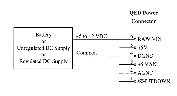
Figure 13.3 shows how to connect a regulated or unregulated DC supply or battery to the power connector of the QED Board. We recommend that any non-battery DC source should be connected to the QED Board via the power connector as shown in Figure 13.3 to take advantage of the onboard surge suppression and EMI filtering circuitry.
To use a battery as a power source, connect the battery's positive terminal to the Raw.Vin input and its negative terminal to the DGND pin at the power connector. These connections are the same as shown in Figure 13.3. You could also connect the battery input to V+raw and DGND at either the Address/Data connector or the Digital I/O connector (see Appendix A for pin locations). This connection scheme bypasses the surge suppression varistor and the EMI filter (see Figure 13.1); this should not pose a problem with battery powered systems because they are unlikely to suffer from power surges or power-induced EMI.
The onboard dual regulator has a very low "dropout" voltage. It can generate regulated 5 Volt outputs from unregulated voltages that are only slightly above 5 Volts. The dropout voltage is 0.6 Volts for +5VAN loads up to 10 mA and +5V loads up to 500 mA. This means that the dual regulator still functions properly when the battery voltage applied to V+raw is as low as 5.6 Volts.
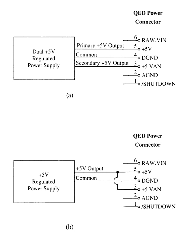
You can bypass the onboard regulation and power the QED Board directly by driving the +5V and +5VAN pins with a regulated +5 Volt power supply. The DGND (digital ground) signal on the QED Board should be connected to the external supply's "return" or "common" output. To maintain separate regulation of the analog circuitry (for low noise operation), two separate five volt sources with a common ground may be used as shown in Figure 13.4(a). Otherwise you may connect a single +5 volt regulated supply to both the +5V and +5VAN pins as shown in Figure 13.4(b). If it is inconvenient to connect to the power connector on the QED Board, you can connect your power source(s) to the +5V, +5VAN, and DGND signals at any of the other connectors at which they appear (see Appendix A for pin locations).
Figure 13.3. Regulated or unregulated DC voltages derived from AC power or from a battery can power the QED Board. The input voltage should be more than 5.6 Volts and less than 14 Volts. Apply the positive voltage to Raw.Vin at pin 6 of the power connector, and the "common" (the battery's negative) voltage to DGND at pin 4 on the power connector.
Figure 13.4. The QED Board may be powered directly by two regulated 5 Volt DC supplies as shown in (a); this maintains a separate supply for onboard analog circuitry. It is also possible to power the board from a single +5 Volt supply by connecting the +5VAN and +5V pins on the power connector as shown in (b).
Making Cable Connections
For those who want to make their own cable to attach to the QED Board's power connector, we recommend using 22 AWG (gauge) wire terminated using Molex crimp-style pins #08-50-0114 and inserted into Molex 6 pin connector housing #22-01-3067. Cable assembly is much easier if you have a ratchet crimp tool to connect the pins to the cable wires. Inexpensive yet functional crimp tools may be purchased at electronics stores such as Radio Shack. Use the crimping tool to connect each cable wire to a Molex crimp-style terminal pin. Then insert the pins at the appropriate locations in the 6 pin housing.
Regulated Supplies For Add-On Boards
Most QED systems consist of a QED Board and one or more custom signal conditioning boards. The components on these add-on boards may be powered either by the available +5V and +5VAN supplies or by a local voltage regulator on each board. Using the QED Board's regulated supplies is simpler, while creating local regulated voltages may result in lower noise and improved modularity.
Add-on boards may be powered by the available +5V and +5VAN supplies as long as their maximum current specifications (750 mA and 10 mA, respectively) are not exceeded, and as long as the input to the regulator is always greater than 5 Volts plus the dropout voltage. Note, however, that additional heat sinking of the QED Board's onboard regulator may be required if significant additional current is drawn from the main +5V supply. The power and ground signals are brought out to most of the QED connectors for your convenience; consult Appendix A for pin assignments.
To maximize reliability and minimize noise, we recommend installing a local voltage regulator on each add-on board in your system. The best way to create a local +5 Volt supply is to regulate the V+raw signal which is brought out to the Address/data, Digital I/O, and Analog I/O connectors. Note that V+raw is not active when the QED Board is powered by an external 5 Volt supply as shown in Figure 13.4.
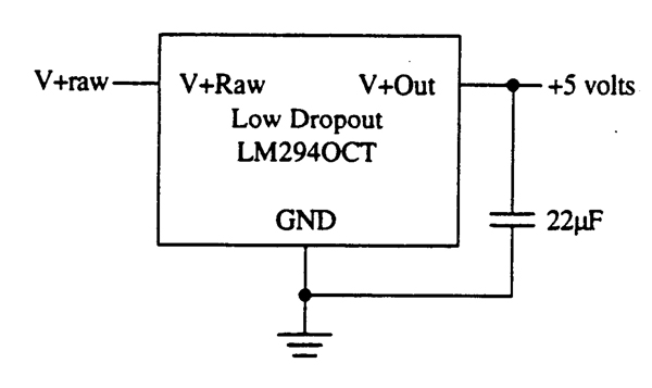
Figures 13.5 and 13.6 show simple circuits that can be implemented on peripheral boards to derive a regulated 5 volt power rail from V+raw. Figure 13.5 shows a low-dropout regulator circuit that can be used when the QED Board is powered by a DC source that is greater than 5 Volts plus the dropout voltage. The dropout voltage ranges from 0.2 Volts to 1 Volt depending on the current being drawn, so DC voltages as low as 5.2 Volts may be used.
Figure 13.5. 5 Volt regulator circuit based on a low-dropout regulator.
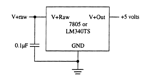
Figure 13.6 shows a standard 5 Volt regulator (7805 or LM340TS) that has a dropout voltage of 2 Volts. This circuit may be used when the QED Board is powered by a DC voltage whose minimum value is greater than 7 Volts.
Figure 13.6. Local 5 Volt regulation circuit based on a standard 5 Volt regulator.
Automatic Generation of Reset and Power-Fail Signals
When the QED Board is powered on, the onboard power monitor circuitry generates the active-low /RESET signal and holds it active (low) until the +5V rail exceeds 4.5 Volts. At this point the /RESET signal is de-asserted, allowing the processor to exit the reset condition and start operating.
When the board is powered down, the +5V power rail is again automatically monitored. When the rail falls to 4.65 Volts, the active low /Power.Fail signal is asserted as explained below. When the positive rail falls below 4.5 Volts, the active-low /RESET signal is asserted. The power monitor's actions preserve the integrity of data in battery-backed RAM as the board is powered up and powered down, and also provide a useful early warning of impending power loss.
Reset Signal
The active-low /RESET signal is very versatile. Normally held high by a pull-up resistor, it can be connected to the reset inputs of hardware devices so that they are reset whenever the power monitor or the reset switch (DIP switch #6) force the /RESET signal low. The /RESET signal is available on both the Address/Data connector and the Digital I/O connector, and peripheral devices can drive it low (using an open collector output) to force all the devices connected to the /RESET line to reset themselves.
The processor's active-low reset pin is attached to the /RESET line. The processor treats the /RESET signal either as an input or an output, depending on the situation. The signal typically acts as a normally-high input that can be driven low by the open-collector output of the power monitor (when the positive supply rail is below 4.5 Volts) or by activating the reset switch.
The processor drives the /RESET line low for less than 4 cycles (2 µsec if the board is clocked at 8 MHz) when a clock monitor failure or computer operating properly (COP) failure occurs (see Chapter 8). This is the processor's way of notifying other peripherals to reset themselves after such an operational failure is detected.
The onboard 82C55A peripheral interface adapter (PIA) chip is reset upon power-up by an active-high RESET output of the power monitor circuitry; this signal is not brought out to the connectors. This hardware PIA reset causes all of the PIA ports to be configured as digital inputs held in a high state. The QED-Forth startup program always reconfigures the PIA such that ports PPA and PPC are inputs held in the high state, and PPB is an output port compatible with the keypad/display interface (see Chapter 2 for more detailed information). Pulling the /RESET signal low does not affect the PIA's active-high RESET signal. Thus the PIA does not receive a hardware reset when the reset button is pushed, but the QED-Forth startup program is always invoked by a reset and configures the PIA as explained above.
Summary
The QED Board can be powered in a variety of ways. The first option is to use a 6 to 12 Volt regulated or unregulated DC source from a voltage supply or battery can be applied to the "Raw.Vin" input (pin 6 of the power connector) with the supply's "return" or "common" connected to the DGND signal (pin 4 of the power connector). A second option is to connect a single regulated +5 Volt supply to both +5V and +5VAN with the common connected to DGND (which is connected to AGND on the board). A third option is to use dual regulated +5 Volt supplies, with one connected to +5V the other connected to +5VAN, and the commons connected to DGND and/or AGND (which are connected together at a single point on the board).
Using option 1 allows you to take advantage of the onboard interference- and surge-suppression circuitry which protects and maximizes the reliability of the circuitry. An alternative form of option 1 is to apply the 6 to 12 Volt external supply to the V+raw pin which is available at the Address/Data and Digital I/O connectors; however, this alternative bypasses the interference- and surge-suppression circuitry.
Two regulated 5 Volt power rails drive the onboard circuitry: a main power rail, +5V, and one used exclusively by the analog references and the 12-bit A/D block, +5VAN. The main +5V supply can source up to 750 mA and can be shut down by an active-low signal called /Shutdown available at the power connector or the Digital I/O connector. The +5VAN supply can source up to 10 mA and is not affected by the /Shutdown input, so it can be used to power circuitry that generate the /Shutdown signal. The dropout voltage for the dual +5 Volt supplies is 0.6 Volts. DGND is the digital ground, and AGND is the analog ground; these grounds are routed separately for maximum noise immunity, and are joined together on the board at a single point. V+raw, +5V, +5VAN, DGND, and AGND are available as either inputs or outputs at various connectors on the board. V+raw is a convenient power source for boards added to the QED system.

