manufacturer of I/O-rich SBCs, operator interfaces, handheld instruments, and development tools for embedded control low cost single board computers, embedded controllers, and operator interfaces for scientific instruments & industrial control development tools for embedded control order our low cost I/O-rich embedded control products embedded controller manufacturer profile single board computers & embedded controllers development tools & starter kits for your embedded design operator interfaces with touchscreens and graphical user interface plug-in expansion modules for digital & analog I/O C language & Forth language integrated development tools, IDE single board and embedded computer accessories embedded controller enclosures, bezels, environmental gaskets

The C Programmer’s Guide to the QVGA Controller

Table of Contents

PART 1 GETTING STARTED

Introduction. How to Use This Manual

Chapter 1: Getting to Know Your QVGA

PART 2 PROGRAMMING THE QVGA CONTROLLER

Chapter 2: Your First Program

Chapter 3: The IDE: Writing, Compiling, Downloading and Debugging Programs

Chapter 4: Making Effective Use of Memory

Chapter 5: Programming the Graphical User Interface

Chapter 6: Real Time Programming

Chapter 7: Failure and Run-Time Error Recovery

PART 3 COMMUNICATIONS, MEASUREMENT, AND CONTROL

Chapter 8: Digital and Timer-Controlled I/O

Chapter 9: Data Acquisition Using the QVGA Controller

Chapter 10: Outputting Voltages with Digital to Analog Conversion

Chapter 11: Serial Communications

Chapter 12: The Battery-Backed Real Time Clock

PART 4: PUTTING IT ALL TOGETHER

Chapter 13: A Turnkeyed Application

PART 5: REFERENCE DATA

Appendix A: QVGA Electrical Specifications
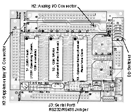
Appendix B: Connector Pinouts

Appendix C: Physical Dimensions

Appendix D: Schematics (pdf)

Appendix B

<< Previous | Next>>

Appendix B: Connector Pinouts

The QVGA Controller comprises a stack of three boards: a display backplane, the QVGA Board, and the smaller QED-4-QVGA Board (aka QED-Flash Board). Pin-outs for all I/O connectors on the QED-Flash Board or the QVGA Board are provided here.

Warning – Do Not Connect to System Control Signals

When connecting to the Digital I/O Connector (H2 on the QVGA Board) with a ribbon cable, notch out cable wires 11 through 24.  Even short pieces of wire connected to some of these lines may cause intermittent operation of the touchscreen or processor.

When connecting to the Supplemental I/O Connector (H3 on the QED Board) with a ribbon cable, only connect the wires you need, and do not connect to the data bus lines or system control lines.

QED Flash Board Connectors

The pinouts of all of the connectors on the QED–Flash Board are presented below.  To locate the connectors on the board, consult Figure B–1  and the white silk–screened labels on the visible side of the QED–Flash Board.  The arrows in the figure point to the locations of pin 1 on each connector.

Figure B–1   QED–Flash Board Connectors and Switches.  Arrows locate pin 1 of each connector.


Table B‑1       H3: Supplemental I/O Connector

Signal


Pins


Signal

PPB4

–

1

2

–

GND

PPB3

–

3

4

–

+5V

PPC3

–

5

6

–

Vcontrast

PPC0

–

7

8

–

A1

PPB2

–

9

10

–

R//W

PPC1

–

11

12

–

Display.E

PPC2

–

13

14

–

D0

PPB1

–

15

16

–

D1

PPB0

–

17

18

–

D2

DGND

–

19

20

–

D3

HC0*

–

21

22

–

D4

HC1 (PB5)*

–

23

24

–

D5

HC2 (PB6)*

–

25

26

–

D6

HC3 (PB7)*

–

27

28

–

D7

DGND

–

29

30

–

DGND

SNUB

–

31

32

–

+5VDD

V+RAW

–

33

34

–

VEE

* HC0 is generated by the PAL, HC1–HC3 are generated from PB5–PB7 respectively.

   You should not connect to the shaded signals. Even a short wire connected to these lines may cause malfunction.


   Table B‑2  H6: Address/Data              Table B‑3  H2: Analog I/O Connector
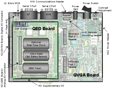
Signal

Pins

Signal


Signal

Pins

Signal

PG7

–

1

2

–

PG6


Vrl

–

1

2

–

Vrh

PG5

–

3

4

–

PG4


PE7/AN7

–

3

4

–

PE6/AN6

PG3

–

5

6

–

PG2


PE5/AN5

–

5

6

–

PE4/AN4

PG1

–

7

8

–

PG0


PE3/AN3

–

7

8

–

PE2/AN2

A15

–

9

10

–

A14


PE1/AN1

–

9

10

–

PE0/AN0

A13

–

11

12

–

A12


12AN7

–

11

12

–

12AN6

A11

–

13

14

–

A10


12AN5

–

13

14

–

12AN4

A9

–

15

16

–

A8


12AN3

–

15

16

–

12AN2

A7

–

17

18

–

A6


12AN1

–

17

18

–

12AN0

A5

–

19

20

–

A4


AGND

–

19

20

–

+5VAN

A3

–

21

22

–

A2


Vin1

–

21

22

–

Vout1

A1

–

23

24

–

A0


Vin2

–

23

24

–

Vout2

D7

–

25

26

–

D6


Vin3

–

25

26

–

Vout3

D5

–

27

28

–

D4


Vin4

–

27

28

–

Vout4

D3

–

29

30

–

D2


Vin5

–

29

30

–

Vout5

D1

–

31

32

–

D0


Vin6

–

31

32

–

Vout6

/RESET

–

33

34

–

R//W


Vin7

–

33

34

–

Vout7

/OE

–

35

36

–

/WE


Vin8

–

35

36

–

Vout8

E

–

37

38

–

V+Raw


1.5Vref

–

37

38

–

+5V

DGND

–

39

40

–

+5V


Analog Bus V–

–

39

40

–

V+Raw

You should not generally need to connect to the processor's address and data bus.  Please consult Mosaic Industries before attempting to connect to these signals.


Processor Port E may be used as either 8–bit A/D inputs (AN0–7) or as digital inputs.  12AN0-7 are 12-bit A/D inputs.  Vin1-8 and Vout1-8 are the 8-bit multiplying DAC inputs and outputs.


QVGA Board Connectors

The pin-outs of all of the connectors on the QVGA Board are presented below.  To locate the connectors on the board, consult Figure B‑2  and the white silk–screened labels on the visible side of the QVGA Board.

Figure B‑2    Connectors and Switches on the QVGA Controller


Table B‑4   H22: Power Header

Signal


Pins


Signal

GND

–

1

2

–

GND

V+Raw

–

3

4

–

V+Bias

+12 V / +5 V ALT

–

5

6

–

+5 V

+5 VAN

–

7

8

–

+3.3 V

MONO_VEE

–

9

10

–

GND


  Table B‑5     Serial 1 Connector                     Table B‑6       Serial 2 Connector

Signal

Pins

Signal


Signal

Pins

Signal

NC

–

1


NC

–

1


6

–

DSR1/DTR1


6

–

DSR2/DTR2

TXD1

–

2


TXD2

–

2


7

–

CTS1


7

–

CTS2/RTS2

RXD1

–

3


RXD2

–

3


8

–

RTS1


8

–

RTS2/CTS2

DSR1/DTR1

–

4


DSR2/DTR2

–

4


9

–

NC


9

–

NC

DGND

–

5


DGND

–

5


Notes:


Notes:

NC indicates no connection


NC indicates no connection

Pins 4 and 6 (DSR1/DTR1) are connected.


Pins 4 and 6 (DSR1/DTR1) are connected.

Pins 7 and 8 (CTS1/RTS1) may optionally be connected on the board with zero ohm shorts.


Pins 7 and 8 (CTS1/RTS1) are connected.


Table B‑7   H14: Serial Communications Connector

Signal


Pins


Signal

TxD1

–

1

2

–

RxD1

DGND

–

3

4

–

DGND

XCVR-

–

5

6

–

XCVR+

TxD2

–

7

8

–

RxD2

DGND

–

9

10

–

DGND


    Table B‑8       Wildcard Port Header

Signal


Pins


Signal

GND

–

1

2

–

+5V

/IRQ

–

3

4

–

V+Raw

PG1/XMIT-

–

5

6

–

PG0/XMIT+

MOSI/XCV-

–

7

8

–

MISO/XCV+

/RESET

–

9

10

–

SCK

/MOD.CS

–

11

12

–

16 MHz

E

–

13

14

–

R/W

/OE

–

15

16

–

/WE

AD7

–

17

18

–

AD6

AD5

–

19

20

–

AD4

AD3

–

21

22

–

AD2

AD1

–

23

24

–

AD0


Table B‑9   H2, H4: Digital I/O Connector

Signal


Pins


Signal

GND

–

1

2

–

+5V

PA7

–

3

4

–

PA6

PA5

–

5

6

–

PA4

PA3

–

7

8

–

PA2

PA1

–

9

10

–

PA0

PD5//SS

–

11

12

–

PD4/SCK

PD3/MOSI

–

13

14

–

PD2/MISO

E

–

15

16

–

R//W

/OE

–

17

18

–

/WE

/XIRQ

–

19

20

–

/IRQ

PFI Input

–

21

22

–

4xOut

/Reset

–

23

24

–

/Shutdown

PPC7

–

25

26

–

PPC6

PPC5

–

27

28

–

PPC4/RS485.XMIT

PPA7

–

29

30

–

PPA6

PPA5

–

31

32

–

PPA4

PPA3

–

33

34

–

PPA2

PPA1

–

35

36

–

PPA0

AGND

–

37

38

–

+5VAN

DGND

–

39

40

–

V+Raw

Notes:

Headers H2 and H4 are connected in parallel.  H4 connects to the QED Board, and H2 is available for you to connect to.

You should not need to connect to the shaded signals.  When connecting a ribbon cable to H2 you should notch out the wires corresponding to the shaded signals, pins 11 through 24.  Even short lengths of wire connected to these signals may cause intermittent operation of the processor or the touchscreen.

<< Previous | Next>>


Home|Site Map|Products|Manuals|Resources|Order|About Us
Copyright (c) 2006 Mosaic Industries, Inc.
Your source for single board computers, embedded controllers, and operator interfaces for instruments and automation