

|
|
Table of ContentsConnecting to the 24/7 Data Acquisition Module Converter Noise and Effective Resolution Other Sources of Noise and Offset Error Tips For Measuring Small Voltages Addressing the 24/7 WildCard Using Module Select Jumpers Initializing the 24/7 Data Acquisition Wildcard Specifying the Reference Voltage Calibration Options Single- and Multi-Channel Sampling Continuous Sampling from a Single Channel |
24/7 Data Acquisition Wildcard Users GuideThere are also input errors contributed by the analog switches. They contribute a maximum of 2.5 nA leakage current at 85 degC. Their leakage is probably insignificant at room temperature. Nevertheless that leakage current times the source resistance will give you an input error (which can be calibrated away at a constant temperature). To use the buffered mode call Buffer_On and to stop using the buffered mode call Buffer_Off. Note that in the buffered mode, the input common mode voltage range is limited to +50 mV to +3.5 V. Our own measurements of the input offsets in the unbuffered mode are provided in the following table: 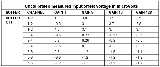 This table was generated by shorting all of the inputs of the AD7714 chip to analog ground. These should be used as a guide for the magnitude of the uncalibrated input offsets – actual values will change from component to component. Converter Noise and Effective ResolutionThe AD7714 data sheet provides the effective resolution of a conversion as a function of gain and sampling frequency in Table Ia (for unbuffered mode) and Table III (for buffered mode) of the AD7714 data sheet. The noise voltages shown on the data sheet result from noise generated internally to the AD7714 chip itself – approximately 1.5 microvolts rms at a 10 Hz sample rate and Gain of 1. The additional circuitry attached to the inputs of the chip contributes additional noise, effectively doubling the noise at low gains. Our own measurements of the rms noise show that it is increased to approximately 2.7 microvoltes at a 10 Hz sample rate and Gain of 1. The noise contribution of the additional circuitry diminishes at greater gains so that the noise figure is dominated by the internally generated noise. Our own measurements of the 24-7 Wildcard Board’s output noise are shown in the following table. Each cell of the table below was calculated by first performing a self calibration and then averaging 100 samples in bipolar mode at 10 Hz. Three sets of measurements were taken for each channel at each gain and the results averaged. 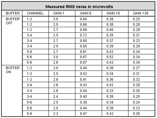 It should be noted that chip’s data sheet defines noise and resolution using rms noise voltages, not peak-to-peak output noise numbers. Peak-to-peak noise numbers can be up to 6.6 times the rms numbers while effective resolution numbers based on peak-to-peak noise can be 2.5 bits below the effective resolution based on rms noise as quoted in the data sheet’s tables. |
Home|Site Map|Products|Manuals|Resources|Order|About Us
Copyright (c) 2006 Mosaic Industries, Inc.
Your source for single board computers, embedded controllers, and operator interfaces for instruments and automation