

|
|
Table of ContentsConnecting to the 24/7 Data Acquisition Module Converter Noise and Effective Resolution Other Sources of Noise and Offset Error Tips For Measuring Small Voltages Addressing the 24/7 WildCard Using Module Select Jumpers Initializing the 24/7 Data Acquisition Wildcard Specifying the Reference Voltage Calibration Options Single- and Multi-Channel Sampling Continuous Sampling from a Single Channel |
24/7 Data Acquisition Wildcard Users GuideAllowable Input ImpedanceIn unbuffered mode there are gain errors owing to the interplay between input impedance, your source resistance and capacitance, and the source resistance and capacitance contributed by protection circuitry we add. Components and transducers with high source impedances connected to the analog inputs will introduce gain errors. Tables XII and XIII in the AD7714 data sheet show the maximum allowable source impedance for there to be no 16- and 20-bit gain errors. These tables are reproduced here: 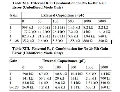 In order to protect the inputs (to ±2000V ESD and ±70V continuously) we add protection resistors and use analog switches and other circuitry to clamp the inputs -- these add a base level of source impedance. The 2.2k protection resistors and the analog switches add additional resistance and capacitance to the inputs, decreasing the amount of allowable impedance listed in Tables XII and XIII. The resistance added is 2.2Kohms and the capacitance added is 22 pF on each line. Looking at Table XII you are allowed a total of 9.6 Kohm of source resistance and 50 pf for no 16-bit errors when using gains of 8-128. Because the protection circuit contributes 2.2K you are really allowed only up to 7.4 K. To allow higher source impedances than those listed in Tables XII and XIII, the analog to digital converter has a buffered mode that buffers the input signal through a unity gain amplifier. The buffered mode operation provides zero gain error at the price of a small dc offset voltage of 2.2 uV. This offset voltage is generated by a 1 nA offset current from the buffer amplifier through the 2.2Kohms protection resistor that is in series with the inputs to the analog to digital converter. To calculate the maximum offset voltage your transducer will generate, use Equation 1. OffsetVoltage(μV)=2.2μV+TransducerSourceImpedance*1nA Equation 1: Calculation of the Offset Voltage in Buffered Mode |
Home|Site Map|Products|Manuals|Resources|Order|About Us
Copyright (c) 2006 Mosaic Industries, Inc.
Your source for single board computers, embedded controllers, and operator interfaces for instruments and automation