manufacturer of I/O-rich SBCs, operator interfaces, handheld instruments, and development tools for embedded control low cost single board computers, embedded controllers, and operator interfaces for scientific instruments & industrial control development tools for embedded control order our low cost I/O-rich embedded control products embedded controller manufacturer profile single board computers & embedded controllers development tools & starter kits for your embedded design operator interfaces with touchscreens and graphical user interface plug-in expansion modules for digital & analog I/O C language & Forth language integrated development tools, IDE single board and embedded computer accessories embedded controller enclosures, bezels, environmental gaskets

QScreen C User Guide

Table of Contents

PART 1 GETTING STARTED

Introduction. How to Use This Manual

Chapter 1: Getting to Know Your QScreen Controller

PART 2 PROGRAMMING THE QSCREEN CONTROLLER

Chapter 2: Your First Program

Chapter 3: The IDE: Writing, Compiling, Downloading and Debugging Programs

Chapter 4: Making Effective Use of Memory

Chapter 5: Real Time Programming

Chapter 6: Failure and Run-Time Error Recovery

PART 3 COMMUNICATIONS, MEASUREMENT, AND CONTROL

Chapter 7: Digital and Timer-Controlled I/O

Chapter 8: Data Acquisition Using Analog to Digital Conversion

Chapter 9: Serial Communications

Chapter 10: The Battery-Backed Real-Time Clock

PART 4: PUTTING IT ALL TOGETHER

Chapter 11: A Turnkeyed Application

PART 5: REFERENCE DATA

Appendix A: QScreen Electrical Specifications

Appendix B: Connector Pinouts

Appendix C: QScreen Schematics

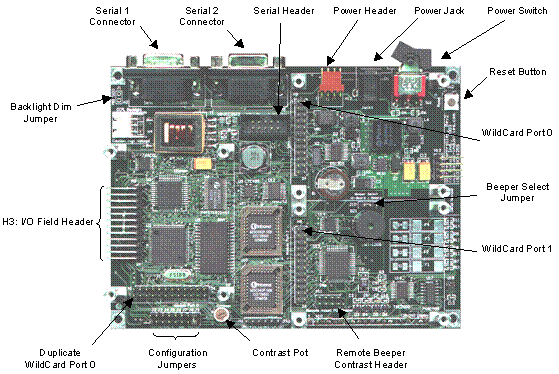
Appendix B

<< Previous | QScreen Schematics

Connector Pinouts

Pin-outs for all I/O connectors on the QScreen are provided here.

QScreen Connectors

The pinouts of all of the connectors on the QScreen Board are presented below.  To locate the connectors on the board, consult Figure B–1  and the white silk–screened labels on the visible side of the QScreen Board.  The arrows in the figure point to the locations of pin 1 on each connector.

Figure B–1   QScreen Connectors, Headers, and Switches. 


Table B‑1     H12: Power Header

Pin


Signal

1

–

Vin

2

–

GND

3

–

+5v

4

–

VBat


Table B‑2     H4: Serial Header

Signal


Pins


Signal

/TxD1

–

1

2

–

/RxD1

GND

–

3

4

–

GND

RS485 XCVR-

–

5

6

–

RS485 XCVR+

/TxD2

–

7

8

–

/RxD2

GND

–

9

10

–

+5V


Table B‑3     H3: Field Header

Signal


Pins


Signal

GND

–

1

2

–

+5V

AGND

–

3

4

–

V+RAW

/TxD1(/TxD2)

–

5

6

–

/RxD1(/RxD2)

XCVR-(TxD2)

–

7

8

–

XCVR+(/RxD2)

PA7

–

9

10

–

PA6

PA5

–

11

12

–

PA4

PA3

–

13

14

–

PA2

PA1

–

15

16

–

PA0

PE7

–

17

18

–

PE6

PE5

–

19

20

–

PE4

PE3

–

21

22

–

PE2

PE1

–

23

24

–

PE0


Table B‑4     H1,H8,H9: Wildcard Port Header

Signal


Pins


Signal

GND

–

1

2

–

+5V

/IRQ

–

3

4

–

V+RAW

SEL1/XMIT1

–

5

6

–

SEL0/XMIT+

MOSI/XCV-

–

7

8

–

MISO/XCV+

/RESET

–

9

10

–

SCK

/MOD.CS

–

11

12

–

16 MHz

E

–

13

14

–

R//W

/OE

–

15

16

–

/WE

AD7

–

17

18

–

AD6

AD5

–

19

20

–

AD4

AD3

–

21

22

–

AD2

AD1

–

23

24

–

AD0


Table B‑5       Serial 1 Connector                     Table B‑6       Serial 2 Connector

Signal

Pins

Signal


Signal

Pins

Signal

DCD1/DSR1/DTR1

–

1


DCD2

–

1


6

–

DSR1/DTR1/DCD1


6

–

DSR2/DTR2/DCD2

/TXD1

–

2


/TXD2

–

2


7

–

CTS1


7

–

CTS2/RTS2

/RXD1

–

3


/RXD2

–

3


8

–

RTS1


8

–

RTS2/CTS2

DSR1/DTR1/DCD1

–

4


DSR2/DTR2/DCD2

–

4


9

–

NC


9

–

NC

DGND

–

5


DGND

–

5


Notes:


Notes:

NC indicates no connection


NC indicates no connection

Pins 1, 4 and 6 (DCD1/DSR1/DTR1) are connected.


Pins 1, 4 and 6 (DCD2/DSR2/DTR2) are connected.

Pins 7 and 8 (CTS1/RTS1) are connected.


Pins 7 and 8 (CTS1/RTS1) are connected.


Table B‑7   H11: Remote Contrast Beeper Header

Signal


Pins


Signal

GND

–

1

2

–

+5V

+5V

–

3

4

–

V+RAW

VCON-

–

5

6

–

VEE

GND

–

9

10

–

REMOTE_BEEPER

<< Previous | QScreen Schematics


Home|Site Map|Products|Manuals|Resources|Order|About Us
Copyright (c) 2006 Mosaic Industries, Inc.
Your source for single board computers, embedded controllers, and operator interfaces for instruments and automation