

|
|
Table of ContentsConnecting To Mosaic Controller Selecting the Wildcard Address Selecting the Reference Voltage Analog I/O Wildcard Field Header Overview of the Software Device Driver Functions Initializing the Analog I/O Software Drivers Installing the Analog I/O Wildcard Driver Software |
Analog I/O Wildcard User GuideConversion AccuracyFor detailed information regarding the converter’s accuracy please consult the datasheet for the ADS8344. In brief, the accuracy and effective resolution of a conversion depends on a number of factors including the converters intrinsic noise and the source impedance. Intrinsic NoiseThe converter exhibits approximately 20 μVrms of effective input noise. When using a reference voltage range of 5 volts, the size of a least significant bit (lsb) is 76 μV, so this input noise corresponds to an error at about the 18 bit level (one quarter of the converter’s lsb), and so does not compromise the performance of the converter. However, if the reference used is only 0.5 V, then the noise corresponds to appx. 3 lsb. Source ResistanceIdeally the converter would be driven by a signal with low source resistance. However, a finite source resistance can compromise the converter’s response via two mechanisms. First, there converter has an input leakage current of as much as ±1μA which flows through the source resistance causing a small input offset voltage. For a source resistance of 100Ω this current causes an offset voltage of 0.1 mV, which corresponds to one and a half counts when using a 5V reference. A greater source resistance would cause a correspondingly greater error; e.g., a 1 KΩ source resistance could produce as much as a ± 13 count error. The input capacitance of the converter must also fully charge through the source resistance during an acquisition time of 2.25μsec. To fully charge, the RC time constant should be much smaller than 2.25μsec. This is usually easily attained. Allowing seven time constants for a large input change to charge with 16-bit precision produces the requirement that 7*RC < 2.25μsec, or R < 2.25 μsec / (7*28pF), or R < 11.5 KΩ. Analog I/O Wildcard Field HeaderThe analog inputs and outputs are brought out to a 24-pin dual row header on the Analog I/O Wildcard as shown in Table 1-5. Table 1-5 Analog I/O Wildcard Field Header 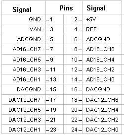 To connect your transducer signals or control inputs to the Field Bus (H3 on the Analog I/O Wildcard) use a ribbon cable or the Screw Terminal Module that brings out the signals to screw terminal blocks. Shielding the connecting wires is highly recommended for optimal performance. |
Home|Site Map|Products|Manuals|Resources|Order|About Us
Copyright (c) 2006 Mosaic Industries, Inc.
Your source for single board computers, embedded controllers, and operator interfaces for instruments and automation