|
|
Table of ContentsSignal Conditioning Wildcard Hardware Connecting an Analog I/O Wildcard to the Wildcard Bus Configuring the Analog I/O Wildcard
Connecting to the Signal Conditioning Wildcard Headers on the Signal Conditioning Wildcard
|
The Signal Conditioning Wildcard User GuideHeaders on the Signal Conditioning WildcardH1 – Input/Output or Field ConnectorThe Field connector is a 24-pin header that you use to connect to your external analog signals. H2 – Analog I/O Field ConnectorThe Analog I/O Field connector is a 24-pin header that you cable to an Analog I/O Wildcard Field header. A 24-pin cable is provided with the Signal Conditioning Wildcard for this purpose. There may be applications for which you do not wish all of the analog inputs/outputs to pass through the Signal Conditioning Wildcard. In that case you can cable only the signals you wish to use, and run other signals directly in/out of the Analog I/O Wildcard as needed. H3 – Wildcard Bus ConnectorThe Wildcard Bus connector is a 24-pin stacking/go through header/socket that allows the Signal Conditioning Wildcard to stack on an Analog I/O Wildcard. Although the Signal Conditioning Wildcard takes its power from this connector, it does not occupy a Wildcard address. Consequently you may use the Signal Conditioning Wildcard without decreasing the number of other Wildcards allowed. The following table describes the signals on each connector: Table 1-1 Signal Conditioning Wildcard Headers
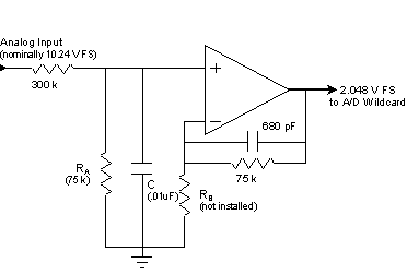
Customizing for Different Full-Scale Voltage RangesThe Signal Conditioning Wildcard has default full scale ranges of 0-20 mA in and out and 0-10V in and out. You can modify these by soldering different components onto the board. Figure 1 shows locations on the board for these components, and it shows which components are installed by default. The following discussion explains which components to change, and how to compute their values, for any full-scale voltage or current range you need. Changing the Input Voltage RangeIn its default configuration the Wildcard accommodates 0–10V full scale input signals. The input voltage is attenuated by a factor of five and filtered by a resistor divider network and presented to a buffer amplifier. The buffer then feeds the resulting 0–2V FS signal to the Analog I/O Wildcard’s A/D converter. You can change the attenuation factor or introduce a gain by changing resistors on the board, and you can change the frequency response by changing a capacitor. A simplified schematic of the circuit is shown in Figure 2. The DC gain of the circuit is given by,
where the resistances are in kΩ. The default configuration is not to install RB and to install 75 kΩ for RA, giving a gain (attenuation) of 0.2. You can change the gain by installing other values. Attenuating Greater Input VoltagesFor example, to operate the circuit as an attenuator for input full scale voltages of any voltage greater than 2.048V you would not install RB, and for RA install a value given by (in kΩ),
For a full scale voltage of 10.24 V this gives the default resistance of 75 kΩ. For a full scale voltage of 100V you would use a resistance of 6.2 kΩ.
Figure 2 The input buffer is programmable for attenuation or amplification. The values installed for a default full-scale input of 10.24 V are shown in parentheses. Amplifying Small Input VoltagesTo amplify signals whose full scale is less than 2.048V, you would not install RA and instead install a value of RB given by (in kΩ),
For example, for a full scale input voltage of 0.1V, RB=3.85 kΩ. Offset and Gain ErrorsIn attenuation mode, the op-amp’s offset error appears as a ±2mV offset on the 2.048V FS signal sent to the A/D. In amplification mode, the op-amp’s offset error is also amplified and is increased to ±2mV*2.048/VinFS. Full scale gain errors result from imprecision in resistor values; when using 1% resistors the full scale gain error is ±1-2%. Adjusting the Anti-Aliasing Low-Pass Filter Cut-Off FrequencyOwing to the capacitors in the input network and in the feedback loop, the circuit acts as an anti-aliasing filter with two low-pass cutoff frequencies. When the circuit amplifies, the feedback loop capacitor causes the gain to drop off with a 3dB cut-off frequency of 3.1 kHz, dropping eventually to unity gain. In either attenuation or gain mode there is an additional low-pass cut-off frequency given by,
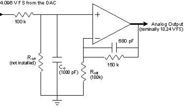
where the frequency is given in kHz for RA in kΩ and C in microfarads. In the default configuration RA = 75 kΩ, C=0.01 μF, and the cut-off frequency is 265 Hz. You can change the cutoff frequency by installing an appropriate value of capacitance. Changing the Output Voltage RangeIn its default configuration, the Wildcard outputs four 0–10.24V output signals. This output is created by amplifying a 0–4.096 voltage range from the Analog I/O Wildcard’s DACs, and buffering it. You can change the gain factor, or attenuate, by changing resistors on the board, and you can change the frequency response of the output by changing a capacitor. A simplified schematic of the circuit is shown in Figure 3:
Figure 3 The output buffer is programmable for attenuation or amplification. The values installed for a default full-scale output of 10.24V are shown in parentheses. The DC gain of the circuit is given by,
where the resistances are in kΩ. The default configuration is to not install RoA and to install 100 kΩ for RoB, giving a gain of 2.5 so that the full scale output is 10.24V. You can change the gain by installing other values. Producing Output Voltages Greater than 4 V Full ScaleFor example, to produce any full scale output voltage greater than 4.096V you would not install ROA, and for RoB install a value given by (in kΩ),
For a full scale voltage of 10.24 V this gives the default resistance of 100 kΩ. For a full scale voltage of 5.12V you would use a resistance of 600 kΩ. Producing Output Voltages Less than 4 V Full ScaleTo produce smaller output voltages, with the full scale output less than 4.096V, you would not install RoB and install a value of RoA given by (in kΩ),
For example, for a full scale output voltage of 1.024V, RoA=33.3 kΩ. Offset and Gain ErrorsIn attenuation mode, the op-amp’s offset error appears as a ±2mV offset on the full scale output voltage. In amplification mode, the op-amp’s offset error is also amplified and is increased to ±2mV* VoutFS /4.096. Full scale gain errors result from imprecision in resistor values, and using 1% resistors the full scale gain error is ±1-2%. Adjusting the Output Low-Pass Filter Cut-Off FrequencyYou can lessen the high frequency content of the output when a step is made, thereby softening the step, by increasing the output filter capacitance. Two capacitors in the buffer produce a two-pole low-pass filter. When the circuit amplifies, the feedback loop capacitor causes the gain to drop off with a 3dB cut-off frequency of 1.6 kHz, dropping eventually to unity gain. In either attenuation or gain mode there is an additional low-pass cut-off frequency given by,
where the frequency is given in kHz for RoA in kΩ and C in microfarads. In the default configuration RoA is not installed (we take the limit of the above equation as RoA goes to infinity), Co=0.001 μF, and the cut-off frequency is 1.6 kHz. You can lower the cutoff frequency further by installing a greater value of capacitance.
| ||||||||||||||||||||||||||||||||||||||||||||||||||||||||||||||||||||||||||||||||||||||||||||||||||||||||||||||||||||||||||||||||||||||||||||||||||||||||||||||||||||||||||||||||||||||||||||||||||||
Home|Site Map|Products|Manuals|Resources|Order|About Us
Copyright (c) 2006 Mosaic Industries, Inc.
Your source for single board computers, embedded controllers, and operator interfaces for instruments and automation